Metal-coated polyimide film and process for producing the same
A technology of polyimide film and manufacturing method, which is applied in metal material coating process, semiconductor/solid-state device manufacturing, sputtering coating, etc. Complicated, copper layer defects and other problems, to achieve the effect of excellent dimensional stability, fewer pores, and high folding resistance
- Summary
- Abstract
- Description
- Claims
- Application Information
AI Technical Summary
Problems solved by technology
Method used
Image

Examples
Embodiment 1
[0094] Hereinafter, it demonstrates step by step.
[0095] 1. Formation of the underlying metal layer (step (a))
[0096] The polyimide film is continuously conveyed by an unwinding machine and a coiling machine, and a nickel-chromium alloy layer with a thickness of 23nm is formed by a common DC sputtering method. The chromium concentration of the nickel-chromium layer was 20% by mass.
[0097] Next, a copper layer with a thickness of 100 nm was formed thereon to obtain an underlying metal layer.
[0098] In addition, the device used to form the underlying metal layer is a device that is equipped with an unwinder, a coiler, and a sputtering device in a vacuum chamber. After the nickel-chromium layer is formed, only the side of the polyimide film is supported by a conveying roller. The coiler coils onto rolls.
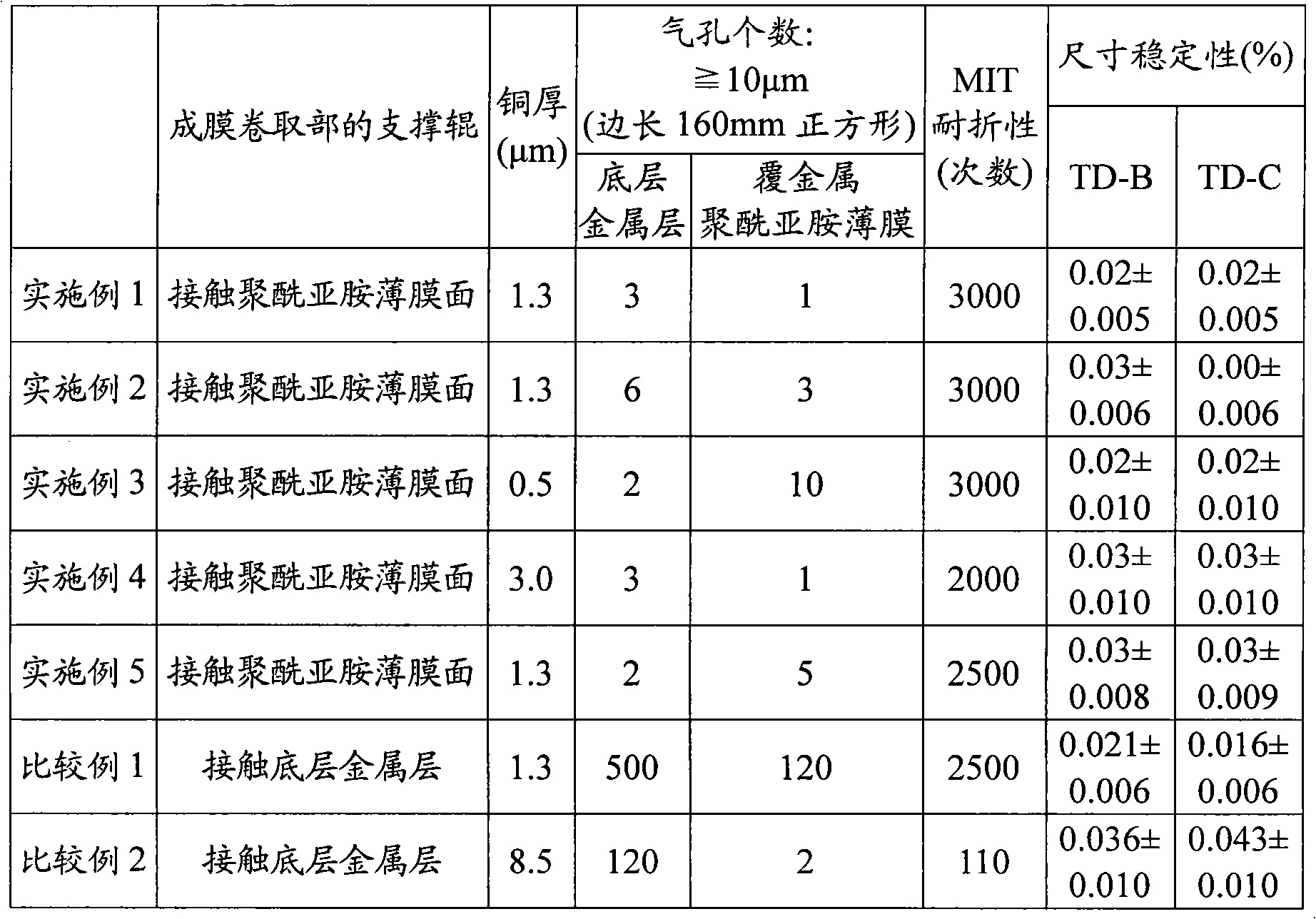
[0099] The results of observing the polyimide film with the underlying metal layer through a light-transmitting observation platform are shown in Table 1.
[0100] ...
Embodiment 2
[0104] Except using a polyimide film with a thickness of 35 μm (manufactured by Kaneka Co., Ltd., Apical-35FP) as the polyimide film, a metal-clad polyimide film was obtained in the same manner as in Example 1, and evaluated in the same manner as in Example 1. . The obtained results are shown in Table 1.
[0105] In addition, the internal stress of the plated film is formed by laminating the film formed by the cell method in the state before the polyimide film is dried, thereby forming a tensile stress corresponding to a range of 5 to 30 MPa.
Embodiment 3
[0107] A metal-clad polyimide film was obtained in the same manner as in Example 1 except that the thickness of the copper plating layer was 0.5 μm, and it was evaluated in the same manner as in Example 1. The obtained results are shown in Table 1.
[0108] In addition, the internal stress of the plated film is equivalent to a tensile stress in the range of 5 to 30 MPa when the film formed by the cell method is stacked in the state before the polyimide film is dried.
[0109] When the previous test piece was measured, the internal stress of the plated film was a tensile stress of 8 MPa in the state before the polyimide film was dried.
PUM
| Property | Measurement | Unit |
|---|---|---|
| thickness | aaaaa | aaaaa |
| thickness | aaaaa | aaaaa |
| thickness | aaaaa | aaaaa |
Abstract
Description
Claims
Application Information
 - R&D
- Intellectual Property
- Life Sciences
- Materials
- Tech Scout
- Unparalleled Data Quality
- Higher Quality Content
- 60% Fewer Hallucinations
Browse by: Latest US Patents, China's latest patents, Technical Efficacy Thesaurus, Application Domain, Technology Topic, Popular Technical Reports.
© 2025 PatSnap. All rights reserved.Legal|Privacy policy|Modern Slavery Act Transparency Statement|Sitemap|About US| Contact US: help@patsnap.com