Pulse coupling based silicon-nanowire complementary metal oxide semiconductors (CMOS) neuronal circuit

A technology of silicon nanowires and pulse coupling, applied in circuits, logic circuits, pulse technology, etc., can solve problems such as difficult to determine network coefficients, uncertain number of iterations, complex pulse threshold processing, etc., to improve computing speed and facilitate information classification Effect

Inactive Publication Date: 2013-06-05
INST OF SEMICONDUCTORS - CHINESE ACAD OF SCI
View PDF1 Cites 0 Cited by
  • Summary
  • Abstract
  • Description
  • Claims
  • Application Information

AI Technical Summary

Problems solved by technology

However, there are still many disadvantages when applying the PCNN network model to image segmentation, such as difficult to determine network coefficients, complex pulse threshold processing, and undetermined number of iterations, etc., especially the pulse threshold in the model is according to the exponential law Attenuation, although this change law is in line with the nonlinear characteristics of the human eye's response to brightness intensity, when computer processing, time needs to be divided into discrete time periods, and the division of time periods not only directly affects the processing speed and segmentation effect

Method used


Image

  • Pulse coupling based silicon-nanowire complementary metal oxide semiconductors (CMOS) neuronal circuit
  • Pulse coupling based silicon-nanowire complementary metal oxide semiconductors (CMOS) neuronal circuit

Examples


Embodiment Construction

[0031] In order to make the object, technical solution and advantages of the present invention clearer, the present invention will be described in further detail below in conjunction with specific embodiments and with reference to the accompanying drawings.

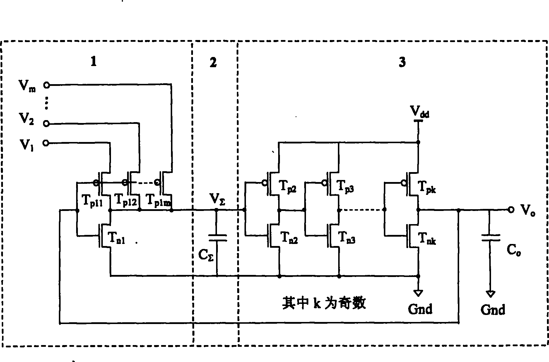
[0032] figure 1 The shown pulse-coupled silicon nanowire CMOS neuron circuit is composed of dendritic circuit 1, integral summer 2 and pulse generating circuit 3 connected in sequence, specifically including:

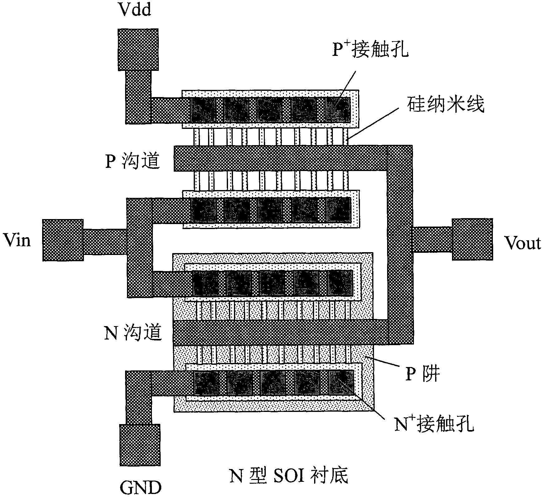
[0033] A dendritic circuit 1, the dendritic circuit 1 is composed of a group of parallel-connected P-type silicon nanowire MOS transistors T p11 ...T p1m with an N-type silicon nanowire MOS transistor T n1 The silicon nanowire CMOS circuit is formed by connecting the drain nodes in series, and the pulse voltage signal is input;

[0034] An integral summer 2, the integral summer 2 is composed of a capacitor C ∑ constituted, the capacitor C ∑ P-type silicon nanowire MOS transistor T in a dendrite circuit p11 .....


PUM


Abstract

The invention discloses a pulse coupling based silicon-nanowire CMOS (complementary metal oxide semiconductors ) neuronal circuit, which consists of a dendrite circuit, an integral summer and a pulse generating circuit, and the dendrite circuit, the integral summer and the pulse generating circuit are sequentially connected. The invention is characterized in that the outputs and inputs of the neuronal circuit are all pulse trains, and the components of the neuronal circuit are all silicon-nanowire CMOS transistors; the dendrite circuit is a CMOS circuit consisting of a set of parallelly-connected P-type nanowire MOS (metal oxide semiconductor ) transistors and an N-type nanowire MOS transistor which are connected in series by drain-terminal nodes, and the source terminals of the P-type nanowire MOS transistors input pulse voltage signals; the integral summer consists of a capacitor C sigma, and the capacitor is connected with the drain-terminal nodes of the P-type and N-type nanowire MOS transistors in the dendrite circuit and used for accumulating and weighting currents so as to form trigger voltage signals; and the pulse generating circuit is a feedback loop consisting of a plurality of even numbered serially-connected CMOS phase inverters and a dendrite CMOS circuit, and used for producing and outputting pulse trains, wherein the output frequency of the pulse trains is modulated by the input voltage pulse signals.

Description

technical field [0001] The invention relates to the technical field of nanometer neuron circuits, in particular to a silicon nanowire CMOS neuron circuit based on pulse coupling. Background technique [0002] Over the past 30 years, integrated circuit technology has developed following Moore's law, and traditional planar CMOS transistors have been scaled down from micrometers to nanometers. Currently, CPU chips based on 45nm gate-length planar CMOS transistors have been commercialized. However, scaling down of planar CMOS devices results in reduced switching performance and increased power density. Low cost, low power consumption, and high integration continue to drive the nanoscale process of CMOS devices. The development of nanometer CMOS transistors from planar structure to three-dimensional nanowire structure has become a trend. Fin-gate silicon nanowire transistors (FinFETs) based on SOI exhibit excellent gate control capability, which is close to the ideal switching ...

Claims


Application Information

Patent Timeline
Patent Type & Authority Patents(China)
IPC IPC(8): H03K19/094H01L27/02
Inventor 韩伟华熊莹赵凯杨香张严波王颖杨富华
Owner INST OF SEMICONDUCTORS - CHINESE ACAD OF SCI
Why Eureka
Try Eureka