High time resolution low noise single photon detector based on optical pulse synchronization

A single-photon detector, high time resolution technology, applied in the direction of instruments, etc., can solve the problems of large post-pulse influence, large time jitter, low signal-to-noise ratio, etc., to improve time resolution, reduce time jitter, and signal synchronization accurate effect

Active Publication Date: 2011-04-06
重庆渝研激光科技有限公司 +1
View PDF6 Cites 12 Cited by
  • Summary
  • Abstract
  • Description
  • Claims
  • Application Information

AI Technical Summary

Problems solved by technology

[0005] Since the gate pulse mode scheme generally adopts the method of increasing the bias voltage and increasing the avalanche amplitude for comparison, the existing problems are: this method cannot control the time jitter of single photon detection, and the implementation of the circuit module is complicated, and the signal-

Method used


Image

  • High time resolution low noise single photon detector based on optical pulse synchronization
  • High time resolution low noise single photon detector based on optical pulse synchronization
  • High time resolution low noise single photon detector based on optical pulse synchronization

Examples


Embodiment 1

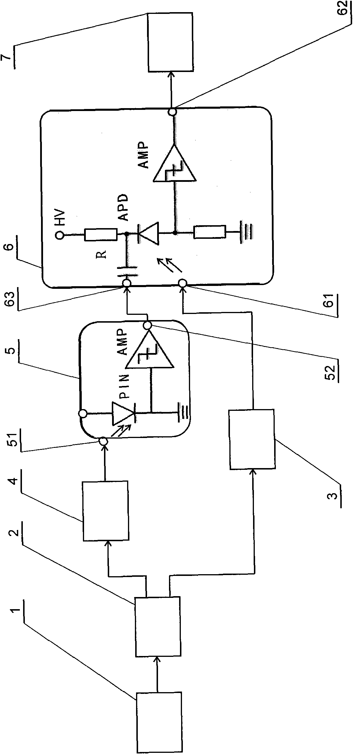
[0018] refer to figure 1 , this embodiment is to load a single Gaussian gate signal to the avalanche diode APD.

[0019] The optical pulse signal sent by the optical pulse generator 1 is divided into two paths by the optical fiber coupler 2, and one path is attenuated by the optical attenuator 3 and then used as incident light by the second optical signal input end 61 of the gate pulse amplification module 6 to enter the avalanche On the diode APD; the other way passes through the optical delay device 4 to control the delay of the optical signal, and the delayed optical signal is incident on the photodiode PIN by the first optical signal input end 51 of the photoelectric conversion module 5, so that it generates a The Gaussian gate pulse electric signal with relatively slow rising and falling edges is amplified by the first amplifier AMP, and the capacitance circuit of the second electric signal input terminal 63 of the gate pulse amplification module 6 and the optical signal ...

Embodiment 2

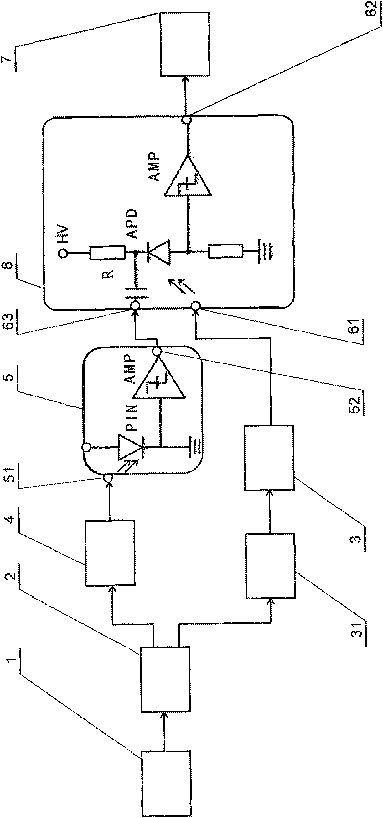
[0021] refer to figure 2 , this embodiment uses re-excitation light as the incident light.

[0022] The excitation light is generated by the optical pulse signal by re-exciting other substances, such as: emittable light, fluorescent light and scattered light as the incident light, which is incident on the avalanche diode APD from the second optical signal input terminal 61 of the gate pulse amplification module 6. The specific process as follows:

[0023] The optical pulse generator 1 sends out an optical pulse signal, which is divided into two paths by the fiber coupler 2, and one path passes through the luminous body 31 to generate excitation light, and after being attenuated by the optical attenuator 3, it is used as the second light by the gate pulse amplification module 6 as the incident light. The signal input terminal 61 is incident on the avalanche diode APD; the other path passes through the optical delay device 4 to control the delay of the optical signal, and the ...

Embodiment 3

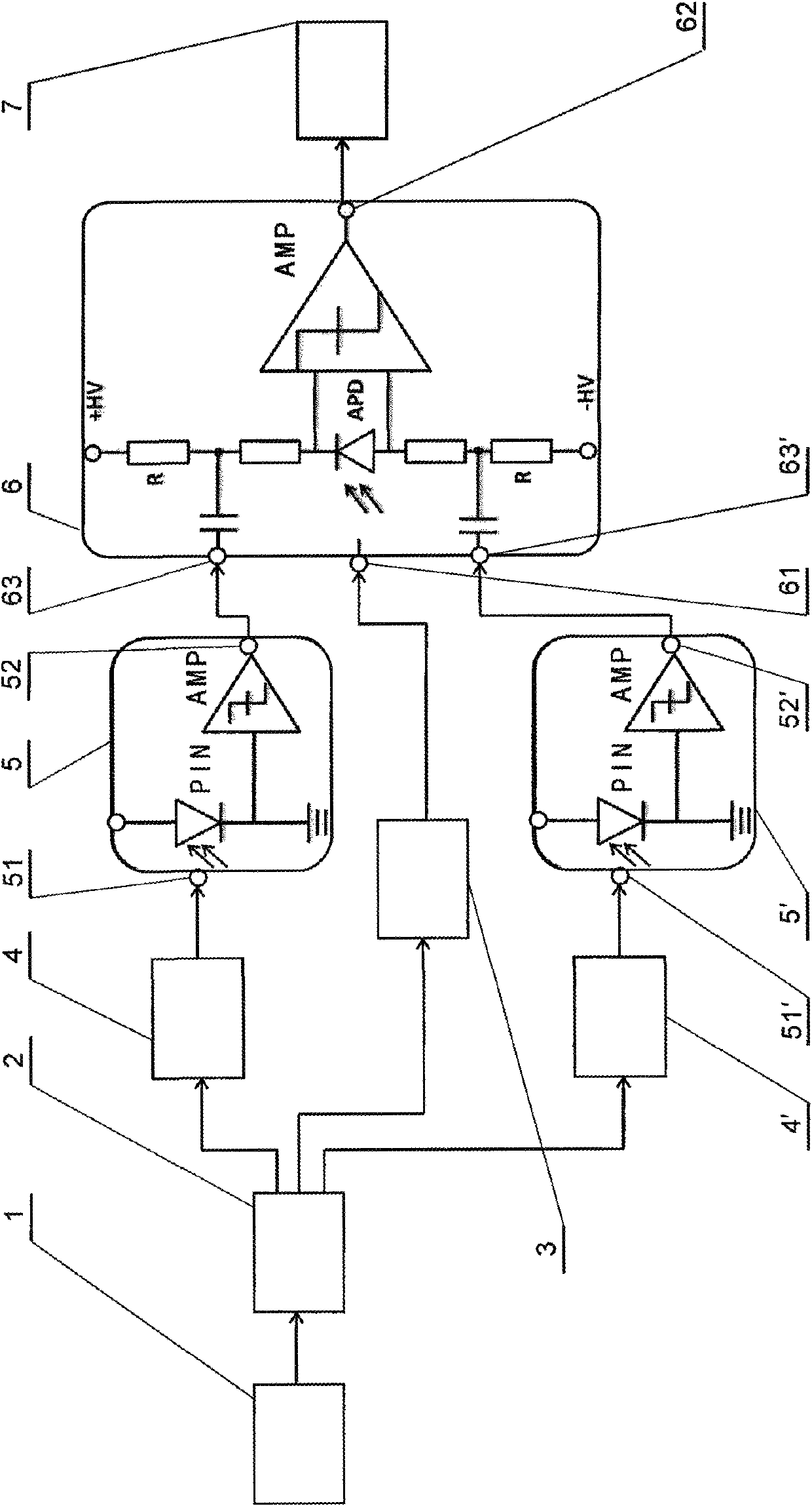
[0025] refer to image 3 In this embodiment, two positive and negative Gaussian gate signals are loaded on the avalanche diode APD at the same time, so that the amplitude of the Gaussian gate pulse can be greatly increased, and the DC high voltage can be reduced and the dark count can be reduced at the same detection efficiency. The specific process is as follows:

[0026]The optical pulse generator 1 sends out optical pulse signals, which are divided into three paths by the optical fiber coupler 2: one path is attenuated by the optical attenuator 3 and then used as incident light by the second optical signal input port 61 of the gate pulse amplification module 6 to enter the avalanche diode On the APD; the other way passes through the optical delay device 4 to control the delay of the optical signal, and the delayed optical signal is incident on the photodiode PIN by the first optical signal input terminal 51 of the photoelectric conversion module 5, so that it generates a ri...


PUM


Abstract

The invention discloses a high time resolution low noise single photon detector based on optical pulse synchronization. The single photon detector comprises an optical pulse generator, an optical fiber coupler, an optical attenuator, an optical delayer, a photoelectric conversion module, a gate pulse amplifier module and a signal extraction module, wherein the optical pulse generator is connected with the optical fiber coupler and divided into two paths, one path is connected with the optical attenuator, the optical attenuator is connected with the optical signal input end of the gate pulse amplifier module, the other path is connected with the optical delayer, the optical delayer is connected with the optical signal input end of the photoelectric conversion module; the output end of the photoelectric conversion module is connected with the electric signal input end of the gate pulse amplifier module; and the electric signal output end of the gate pulse amplifier module is connected with the signal extraction module. The single photon detector uses the optical delayer and the photoelectric conversion module to convert the optical signals to Gaussian electric signals which are used as gate pulse signals, thus the noise of the avalanche photo diode (APD) caused by capacitance effect can be reduced and the signal-to-noise ratio can be increased.

Description

technical field [0001] The invention relates to a detector for high-speed quantum secret communication in the technical field of optical fiber communication, in particular to a high-time-resolution and low-noise single-photon detector synchronized with optical pulses. Background technique [0002] Since quantum secure communication can provide a more secure communication channel, it is of great significance in the fields of national defense, military, political, financial and other communications. Developed countries such as Europe, the United States and Japan are constantly exploring the practical application of quantum secure communication. Switzerland is even using quantum secure communications to help secure voting in general elections. [0003] my country also attaches great importance to the practical application of quantum communication and lists it as a key scientific research project for research. A key technology in the quantum secure communication system is to re...

Claims


Application Information

Patent Timeline
IPC IPC(8): G01J11/00
Inventor 曾和平梁焰
Owner 重庆渝研激光科技有限公司
Why Eureka
Try Eureka