ROM layout method and system

A technology of read-only memory and layout method, which is applied in the field of read-only memory devices and memory devices, can solve problems such as device degradation, and achieve the effect of reducing the effect of device degradation

Active Publication Date: 2014-05-07
TAIWAN SEMICON MFG CO LTD
View PDF4 Cites 0 Cited by
  • Summary
  • Abstract
  • Description
  • Claims
  • Application Information

AI Technical Summary

Problems solved by technology

However, these conventional layouts are limited by the long OD (LOD) effect, polysilicon spacing effect (PSE), and defined oxide spacing effect (OD spacing effect, OSE), all of which can cause device deterioration

Method used


Image

  • ROM layout method and system
  • ROM layout method and system
  • ROM layout method and system

Examples


Embodiment Construction

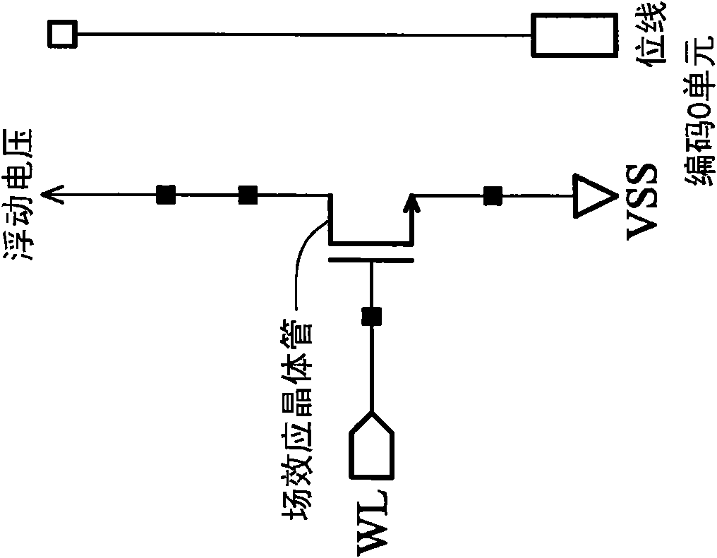
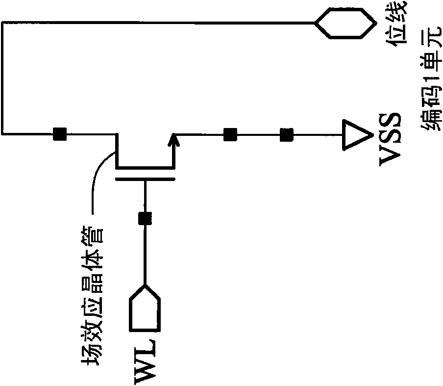
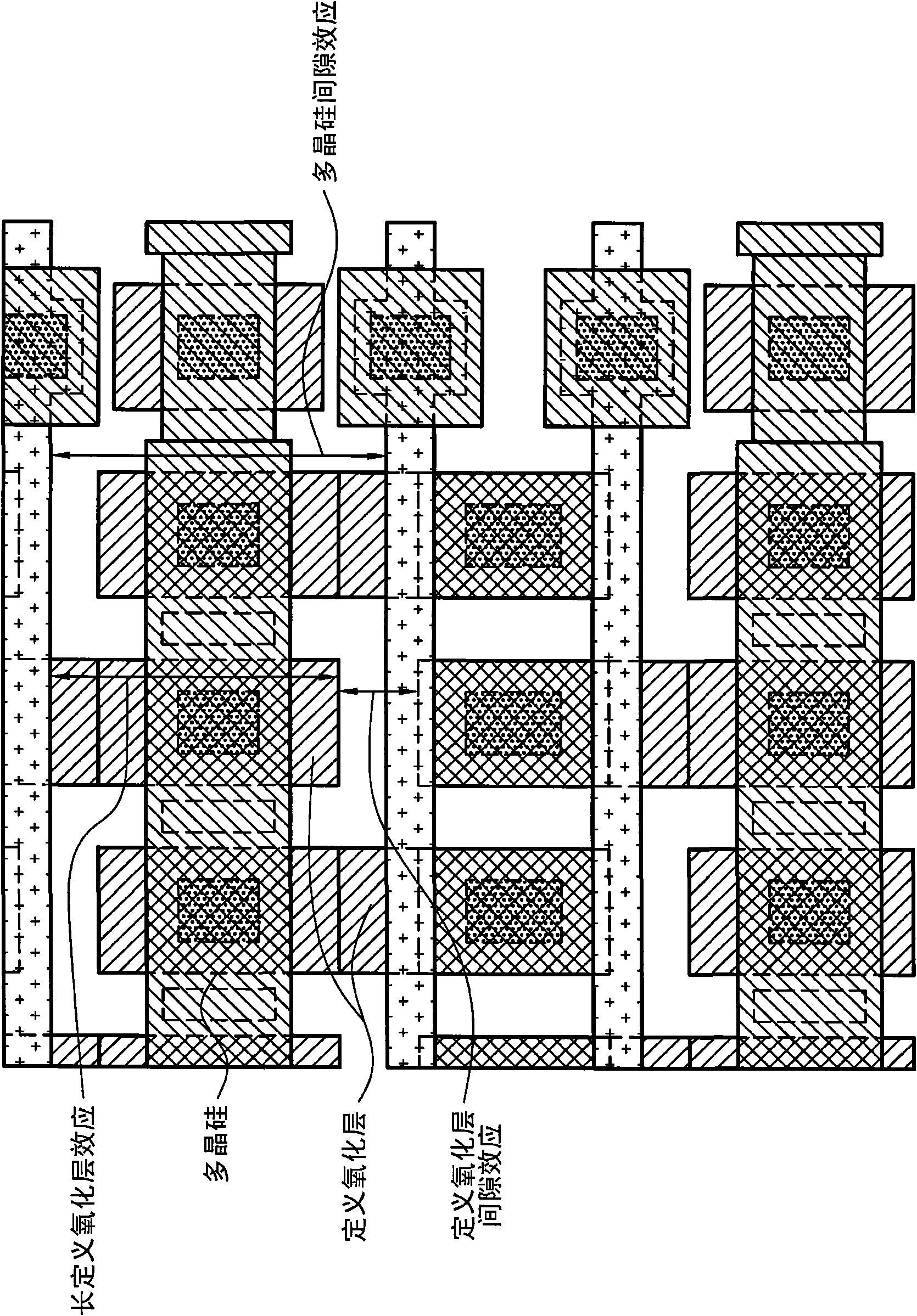
[0048] In previous technologies (eg, sub-32nm technologies), the defined oxide islands can be replaced by redundant devices consisting of continuous defined oxide (continuous OD) and grounded polysilicon to allow equal clearance for Limit the degradation caused by the long definition oxide effect, polysilicon gap effect, and definition oxide gap effect mentioned above. exist image 3One embodiment is shown, a bit cell layout with a continuously defined oxide layer and uniform poly spacing. Grounded polysilicon (e.g., a polysilicon gate coupled to ground) is often used as a redundant device in sub-32nm technology to separate bit-for-bit to avoid shorting of bit cells (e.g., shorting of a coded 1 bit cell to a coded 0 bit cell, and vice versa). These redundant devices are used when the defined oxide layer no longer configures isolated islands.

[0049] However, modeling this grounded polysilicon redundant device using a continuously defined oxide layer in a circuit diagram cr...


PUM


Abstract

A method includes receiving instructions for designing a ROM array, generating netlists for the ROM array, generating a data file representing a physical layout of the ROM array on a semiconductor wafer, and storing the data file in a computer readable storage medium. The instructions for the ROM array define a layout for a first unit including a first bit cell coupled to a first word line, a bus that may be coupled and uncoupled to a first power supply having a first voltage level, a layout for a second unit coupled to a second word line, and a layout for a third unit having an isolation device and being configured to share a bit line contact with the second unit or another third unit. The layout for the second unit is configured to be arranged at an edge of the ROM array and includes a dummy device.

Description

technical field [0001] The system and method disclosed in the present invention mainly relate to a memory device, in particular to a read only memory (ROM) device. Background technique [0002] Currently, bit cell tiling for arbitrary code in ROMs is accomplished by tiling basic code0 cells (code0 cells) and / or code1 cells (code1 cells). Figure 1A as well as Figure 1B It is a design circuit diagram showing code 0 and code 1 bit cells respectively. like Figure 1A As shown, a coding 0 cell is usually implemented with a single field effect transistor (MOSFET) having a gate electrically connected to a word line (WL) and a coding node electrically connected ) of the drain. The bit line (BL) of the coding 0 node is set with a floating voltage to represent a logic zero (logic zero). like Figure 1B As shown, a code 1 cell also includes a field effect transistor having a source coupled to a voltage Vss and a gate electrically connected to a word line. The drain of the field ...

Claims


Application Information

Patent Timeline
Patent Type & Authority Patents(China)
IPC IPC(8): G11C16/06G06F17/50
CPCH01L27/112H01L27/0207H01L27/11226H10B20/34H10B20/00
Inventor 杨振麟
Owner TAIWAN SEMICON MFG CO LTD
Why Eureka
Try Eureka