A pixel driving circuit, array substrate and liquid crystal display device
A pixel driving circuit and pixel electrode technology, which is applied in the fields of pixel driving circuits, array substrates and liquid crystal display devices, can solve problems such as affecting the normal display of display modules, transistor deterioration, etc., so as to reduce the impact of deterioration, reduce leakage current, and increase switching. The effect of circuit resistance
- Summary
- Abstract
- Description
- Claims
- Application Information
AI Technical Summary
Problems solved by technology
Method used
Image
Examples
Embodiment 1
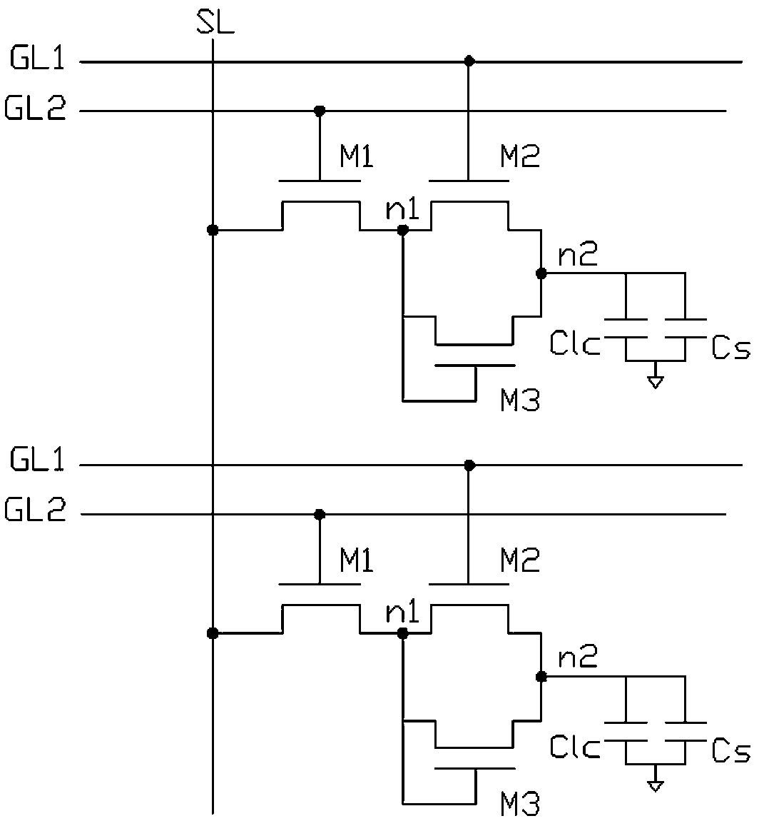
[0018] figure 1 It shows a pixel driving circuit of a preferred embodiment of the present invention, which is used in a liquid crystal display device, including the first gate line Gate Line 1 (GL1), the second gate line Gate Line 2 (GL2), and the data line Source Line (SL), a first transistor M1 , a second transistor M2 , a third transistor M3 and a pixel electrode.
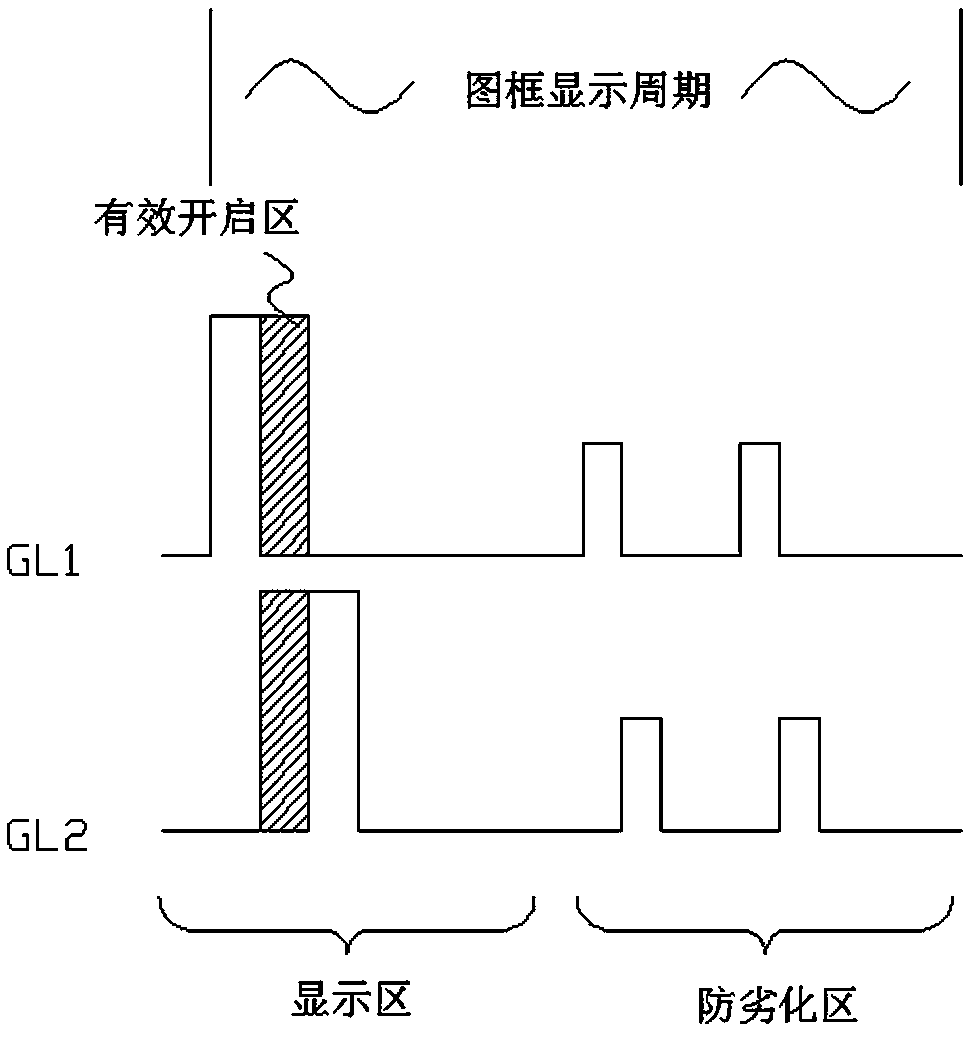
[0019] The first transistor M1 is controlled in response to the second gate signal from the second gate line Gate Line 2 (GL2), and the first transistor M1 is connected to the data line Source Line (SL) and the first node Between n1, that is, the first transistor M1 is turned on or off according to the logic state of the second gate signal, and the data line SL and the first node n1 are electrically connected to each other when the first transistor M1 is turned on. The first transistor M1 has a gate terminal connected to the second gate line GL2, a source terminal connected to the data line SL, and a drain term...
Embodiment 2
[0028] An array substrate, which includes several pixel units distributed in a matrix, and also includes the pixel driving circuit as described in Embodiment 1.
[0029] The array substrate of this embodiment, through the structure of three transistors, can increase the resistance of the switch circuit, reduce the leakage current, facilitate the maintenance of the display picture, and reduce the deterioration effect on the transistor under the low frequency driving signal. In the anti-deterioration area, use the normal driving frequency (such as 60Hz) to turn on one of the transistors independently, which can prevent the transistor from deteriorating, and at the same time, the transistor can also be turned off to prevent pixel leakage and will not affect the display quality.
Embodiment 3
[0031] A liquid crystal display device, comprising the array substrate as described in Embodiment 2. Specifically, the liquid crystal display device may be any product or component with a display function such as a liquid crystal panel, a mobile phone, a tablet computer, a television set, a display area, a notebook computer, a digital photo frame, and a navigator. The display mode of the liquid crystal display device is any one of a normally positive display mode, a normally black display mode, a transmissive mode, a transflective mode, and a full inversion mode.
[0032] The liquid crystal display device of this embodiment, through the structure of three transistors, can increase the resistance of the switch circuit, reduce the leakage current, facilitate the maintenance of the display screen, and reduce the deterioration effect on the transistor under the low frequency driving signal. In the anti-deterioration area, use the normal driving frequency (such as 60Hz) to turn on ...
PUM
 Abstract
Description
Claims
Application Information

