Method and device for protecting silicon wafer edge

A silicon chip edge protection and edge protection technology, which is applied in the field of integrated circuit manufacturing, can solve problems such as low efficiency, and achieve the effects of reduced procedures, low cost, and easy online implementation

Active Publication Date: 2011-04-13
SHANGHAI MICRO ELECTRONICS EQUIP (GRP) CO LTD
View PDF3 Cites 31 Cited by
  • Summary
  • Abstract
  • Description
  • Claims
  • Application Information

AI Technical Summary

Problems solved by technology

relatively l

Method used


Image

  • Method and device for protecting silicon wafer edge
  • Method and device for protecting silicon wafer edge
  • Method and device for protecting silicon wafer edge

Examples


Embodiment Construction

[0050] In order to better understand the technical content of the present invention, specific embodiments are given together with the attached drawings for description as follows.

[0051] The invention provides a method and device for protecting the edge of a silicon chip, which protects the edge of the silicon chip when it is exposed, and does not need to go through two processes to process the edge of the silicon chip, thereby reducing the number of processes and improving production efficiency.

[0052] The present invention determines the method that negative glue exposure and edge protection carry out synchronously, realizes silicon chip edge protection with a kind of mechanical method, to realizing negative glue process exposure process silicon chip edge protection function, comprises the following steps:

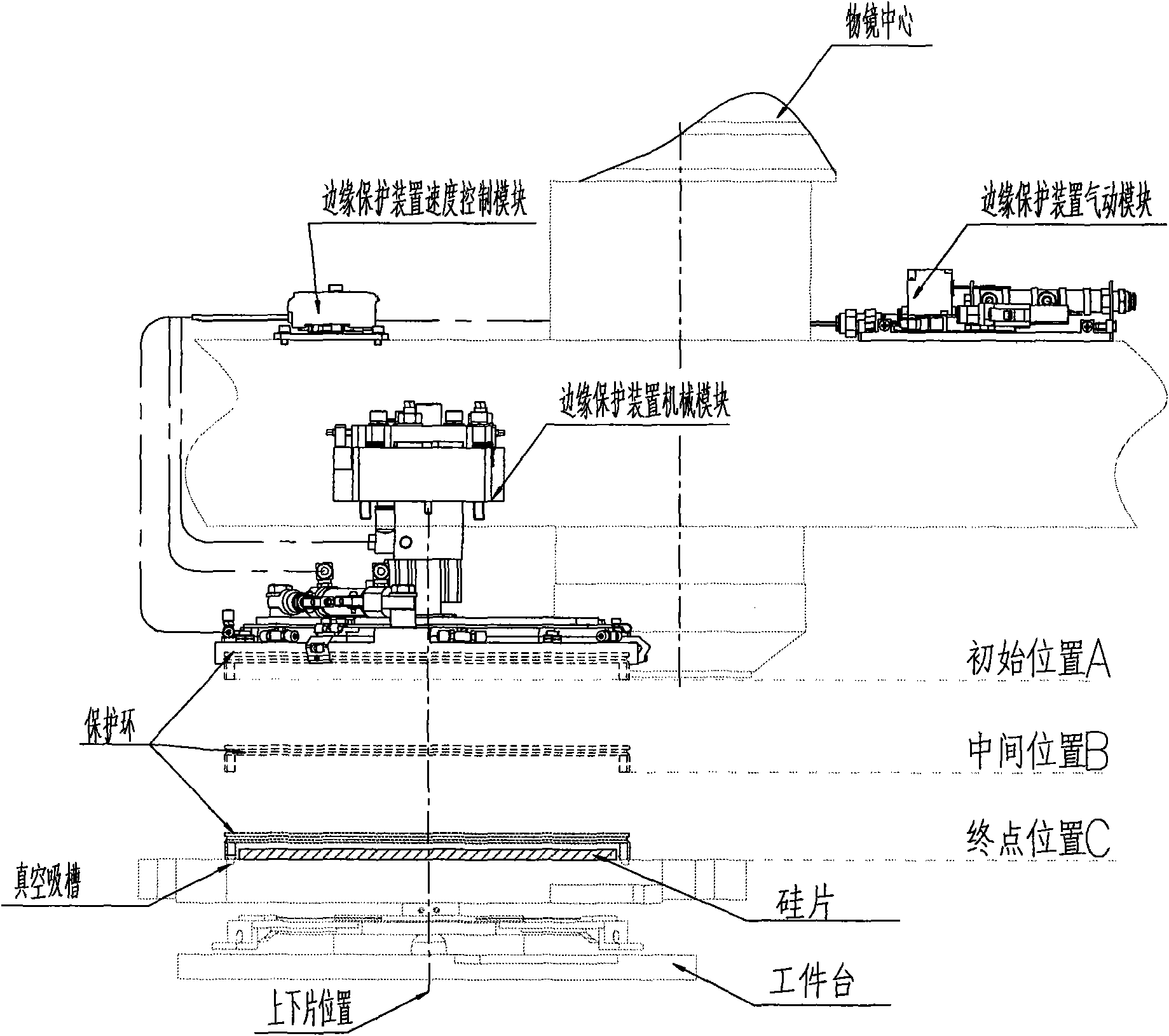
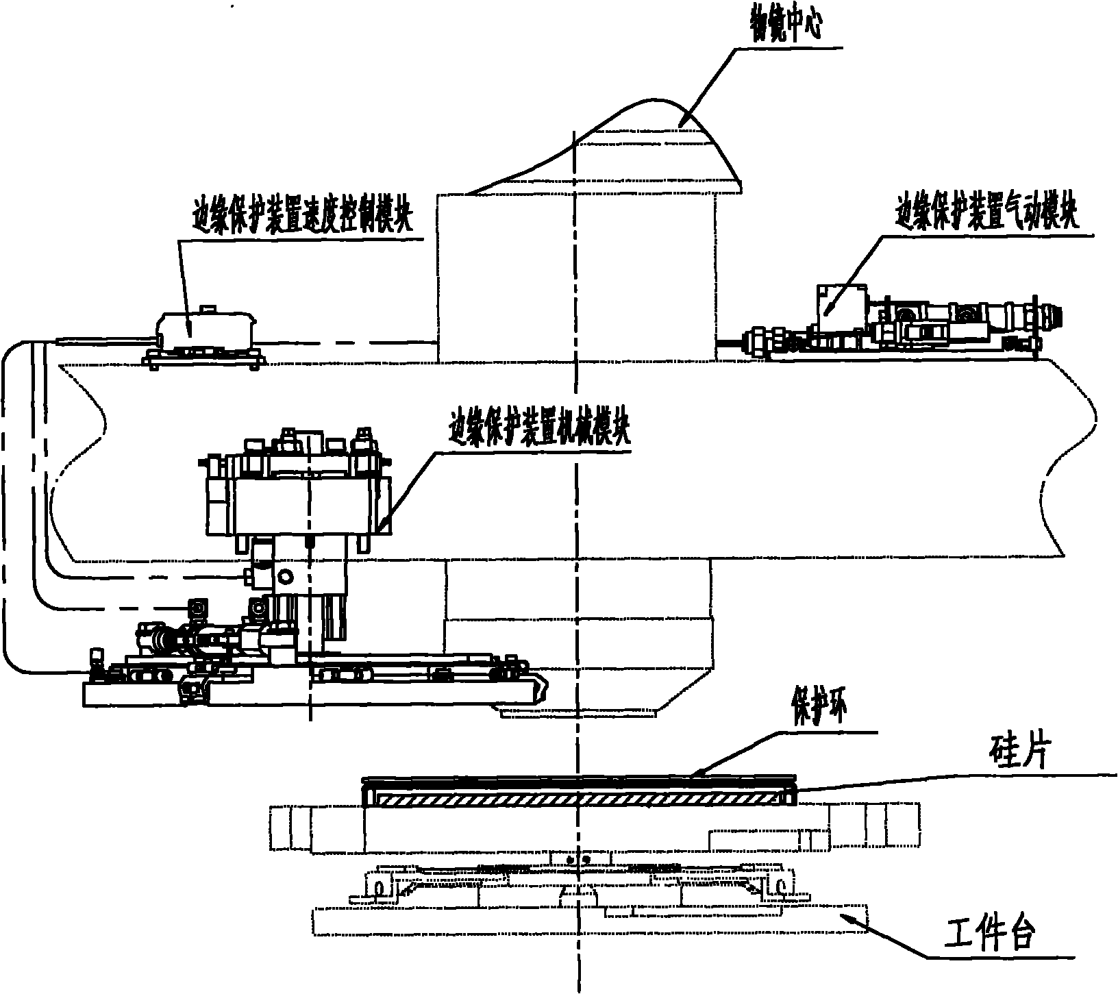
[0053] Use the silicon wafer edge protection device to place the protective ring on the workpiece table where the silicon wafer is placed before the objective lens is...


PUM


Abstract

The present invention provides method and device for protecting silicon wafer edge, wherein the method comprises the following steps: placing a protection ring on a working bench by a device for protecting silicon wafer; protecting the silicon wafer edge by the protection ring during exposure of the silicon wafer; performing said flows again after replacing a new silicon wafer, wherein the centreof the protection ring is a hollow part, and the edge thereof is an entity part; the protection ring prevents the silicon wafer edge from exposing during exposure. The method for protecting silicon wafer edge comprises a position adjusting mechanism, a Z-direction lifting gear, three eccentric linkage overload protection cam-reciprocating pneumatic swing-cylinder connecting rod mechanisms, a blowing mechanism, a detection mechanism, a speed control module, and a pneumatic control module. In the method and device for protecting silicon wafer edge of the present invention, the method is that negative glue exposure and the edge protection are performed synchronously; when the silicon wafer is exposed, the silicon wafer edge is protected without a second process for processing the silicon wafer edge; the processes are reduced, and working efficiency is improved.

Description

technical field [0001] The invention relates to the field of integrated circuit manufacturing, and in particular to a silicon chip edge protection method and device. Background technique [0002] Lithography equipment is mainly used in the manufacture of integrated circuits IC or other micro-devices. With a photolithographic apparatus, a mask pattern can be imaged on a photoresist-coated wafer, such as a semiconductor or an LCD panel. The lithography device exposes through the projection objective lens and transfers the designed mask pattern to the photoresist. As the core component of the lithography device, the edge protection of the silicon wafer has an important impact on the realization of the edge protection function of the silicon wafer during the exposure process of the negative resist process. . [0003] In order to obtain the imaging effect, the photoresist is coated on the silicon wafer, and a photosensitive material that can produce corrosion patterns after exp...

Claims


Application Information

Patent Timeline
IPC IPC(8): G03F7/20
Inventor 吴荣基朱岳彬
Owner SHANGHAI MICRO ELECTRONICS EQUIP (GRP) CO LTD
Why Eureka
Try Eureka