Method for treating groove and forming UMOS (U-shaped groove Metal Oxide Semiconductor) transistor

A technology of transistors and trenches, applied in semiconductor/solid-state device manufacturing, electrical components, circuits, etc., can solve problems such as uneven thickness and unsuitability of UMOS transistors, and achieve the effects of improving flatness, overcoming surface defects, and increasing thickness

Inactive Publication Date: 2011-04-13
SEMICON MFG INT (SHANGHAI) CORP +1
View PDF1 Cites 13 Cited by
  • Summary
  • Abstract
  • Description
  • Claims
  • Application Information

AI Technical Summary

Problems solved by technology

The technical solution of the above-mentioned Chinese patent application 200710044802.2 has been improved for the conventional MOS transistor structure, w...

Method used


Image

  • Method for treating groove and forming UMOS (U-shaped groove Metal Oxide Semiconductor) transistor
  • Method for treating groove and forming UMOS (U-shaped groove Metal Oxide Semiconductor) transistor
  • Method for treating groove and forming UMOS (U-shaped groove Metal Oxide Semiconductor) transistor

Examples


Embodiment Construction

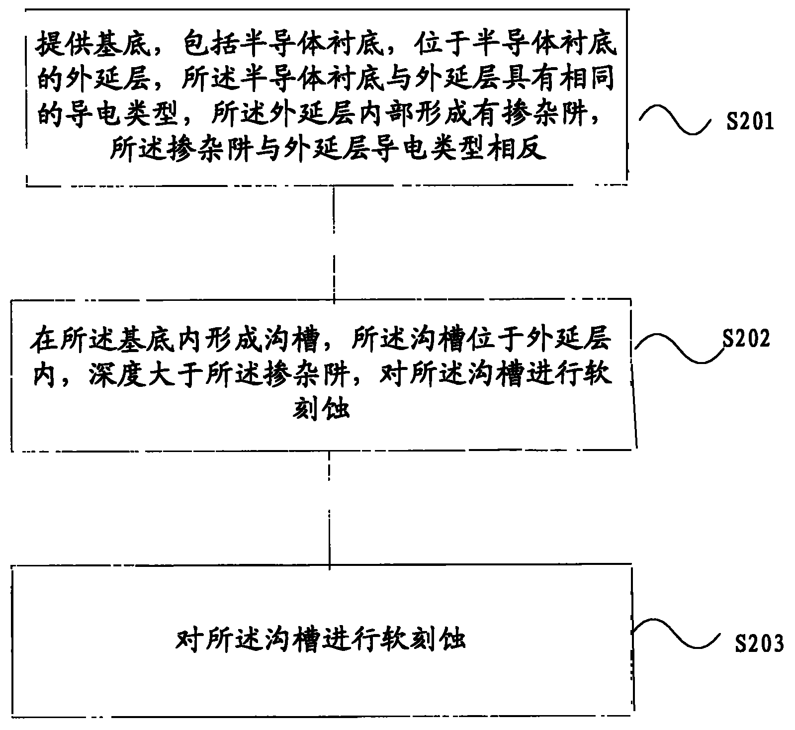
[0026] In order to make the above objects, features and advantages of the present invention more clearly understood, the specific embodiments of the present invention will be described in detail below with reference to the accompanying drawings.

[0027] In the following description, specific details are set forth in order to provide a thorough understanding of the present invention. However, the present invention can be implemented in many other ways different from those described herein, and those skilled in the art can make similar promotions without departing from the connotation of the present invention. Accordingly, the present invention is not limited by the specific implementations disclosed below.

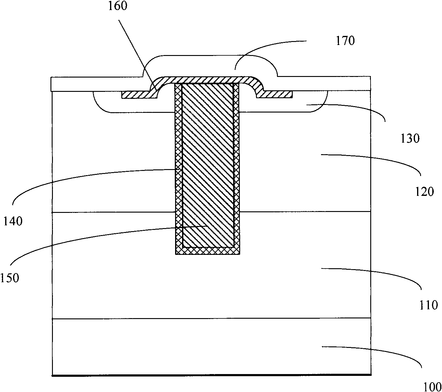
[0028] The method provided by the present invention is not only applicable to power devices, but also applicable to general logic devices and storage devices. It is especially suitable for MOS transistors with a trench gate structure with a feature size of 0.3 μm and belo...


PUM


Abstract

The invention relates to a method for treating a groove and forming a UMOS (U-shaped groove Metal Oxide Semiconductor) transistor, wherein the method for treating the groove comprises the step of carrying out soft lithography on the groove. The invention improves the uniformity of the dielectric layers of the side wall and the bottom of the groove; the process complexity is not increased obviously, and the production cost and the capacity are not changed obviously.

Description

technical field [0001] The present invention relates to the field of semiconductor manufacturing, in particular to a method for processing trenches and forming UMOS transistors Background technique [0002] With the rapid development of semiconductor technology, the manufacturing process of integrated circuits has become more and more complex and sophisticated. In order to improve the integration level, reduce the manufacturing cost, and speed up the operation speed of the semiconductor device, the critical dimension of the semiconductor device is constantly getting smaller. Among various basic semiconductor devices, metal oxide field effect transistors (MOSFETs, MOS transistors for short) are one of the basic units of integrated circuits, and are widely used in various ultra-large-scale storage and logic circuits. [0003] A typical MOS transistor structure includes a source electrode, a drain electrode, a gate dielectric layer, and a conductive gate (gate) located on the ...

Claims


Application Information

Patent Timeline
IPC IPC(8): H01L21/302H01L21/306H01L21/336
Inventor 湛兴龙刘喻韩永召陈建利蔡信裕
Owner SEMICON MFG INT (SHANGHAI) CORP
Why Eureka
Try Eureka