Group iii nitride semiconductor light-emitting device
一种氮化物半导体、发光器件的技术,应用在半导体器件、电固体器件、电气元件等方向,能够解决光提取性能低下等问题
- Summary
- Abstract
- Description
- Claims
- Application Information
AI Technical Summary
Problems solved by technology
Method used
Image

Examples
Embodiment approach 1
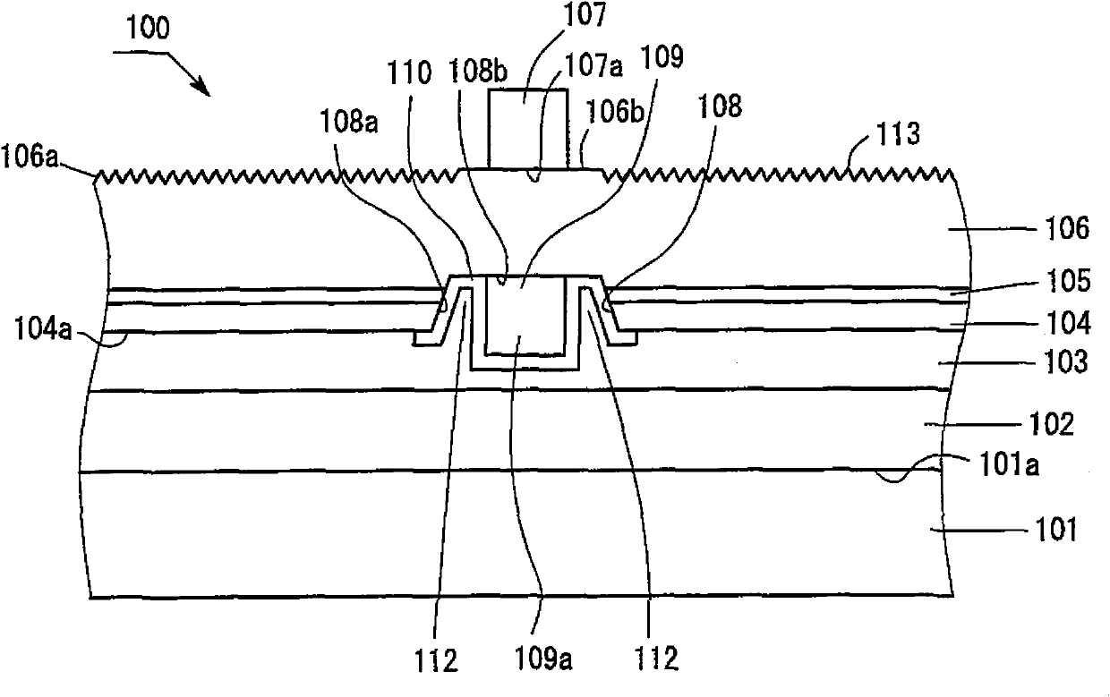
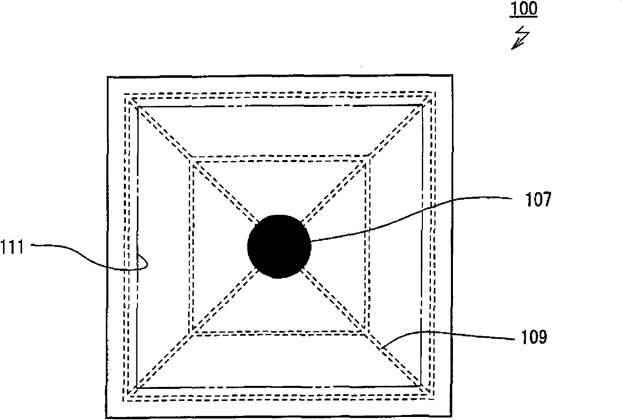
[0082] figure 1 is a cross-sectional view of the structure of the light emitting device 100 according to Embodiment 1, figure 2 is a top view of the light emitting device 100 . like figure 2 As shown, the light emitting device 100 has a square shape viewed from above. like figure 1 As shown, the light-emitting device 100 includes a substrate 101; a low-melting-point metal layer 102 formed on the substrate 101; a p-electrode 103 bonded to the substrate 101 via the low-melting-point metal layer 102; - p-type layer 104 , active layer 105 and n-type layer 106 on electrode 103 ; and n-electrode 107 formed on n-type layer 106 .
[0083] The base 101 may be a conductive substrate formed of, for example, Si, GaAs, Cu, or Cu—W. The low melting point metal layer 102 may be a eutectic metal layer, such as an Au—Sn layer, Au—Si layer, Ag—Sn—Cu layer or Sn—Bi layer. Alternatively, the low melting point metal layer 102 may be, for example, an Au layer, a Sn layer, or a Cu layer, alt...
Embodiment approach 2
[0115] In Embodiment 2, components having the same functions as those described in Embodiment 1 are denoted by the same reference numerals. Figure 9 is a top view of a light emitting device 600 according to Embodiment 2, Figure 10 Yes Figure 9 A cross-sectional view of the device taken along line A-A. like Figure 9 As shown, the light emitting device 600 has a square shape viewed from above. like Figure 10 As shown, the light-emitting device 600 includes a substrate 101; a low-melting-point metal layer 102 formed on the substrate 101; a p-electrode 103 bonded to the substrate 101 via the low-melting-point metal layer 102; - p-type layer 104, active layer 105 and n-type layer 106 on electrode 103; n-pad electrode 607; and auxiliary electrode 609.
[0116] The base 101 may be a conductive substrate formed of, for example, Si, GaAs, Cu, or Cu—W. The bottom electrode 117 is formed on the bottom surface 101b of the substrate 101 (i.e., the surface on the side opposite to...
Embodiment approach 3
[0140] In Embodiment 3, components having the same functions as those described in Embodiment 1 or 2 are denoted by the same reference numerals. Figure 15 is a top view of a light emitting device 700 according to Embodiment 3, Figure 16 Yes Figure 15 A cross-sectional view of the device taken along line A-A. like Figure 16 As shown, the light emitting device 700 includes a ceramic substrate 701; a low melting point metal layer formed on the ceramic substrate 701; a p-electrode 103 bonded to the ceramic substrate 701 via the low melting point metal layer 102; formed of a group III nitride semiconductor And p-type layer 104 , active layer 105 , and n-type layer 106 ; n-pad electrode 707 ; auxiliary electrode 709 and p-pad electrode 714 are sequentially stacked on p-electrode 103 . like Figure 15 As shown in , the light emitting device 700 has a square shape viewed from above, and the n-pad electrode 707 and the p-pad electrode 714 are formed on the same surface.
[014...
PUM
 Abstract
Description
Claims
Application Information
 - R&D
- Intellectual Property
- Life Sciences
- Materials
- Tech Scout
- Unparalleled Data Quality
- Higher Quality Content
- 60% Fewer Hallucinations
Browse by: Latest US Patents, China's latest patents, Technical Efficacy Thesaurus, Application Domain, Technology Topic, Popular Technical Reports.
© 2025 PatSnap. All rights reserved.Legal|Privacy policy|Modern Slavery Act Transparency Statement|Sitemap|About US| Contact US: help@patsnap.com