Array of graphene-based nano-scale point sources

A nanoscale, point light source technology, applied in the field of arrays of nanoscale point light sources, can solve the problems of difficult control of carbon nanotube manufacturing and integration, difficult light source technology, etc., achieve good light intensity control function, and improve light source irradiation range , the effect of high integration

Active Publication Date: 2011-04-27
SEMICONDUCTOR MANUFACTURING INTERNATIONAL (BEIJING) CORP +1
View PDF3 Cites 4 Cited by
  • Summary
  • Abstract
  • Description
  • Claims
  • Application Information

AI Technical Summary

Problems solved by technology

In addition, although there are reports of nano light sources based on carbon nanotubes (J.A.Misewich, et al.Science, 300, 783 (2003), Dingshan Yu and LimingDai, Appl Phys Lett 96, 143107 (2010)), du

Method used


Image

  • Array of graphene-based nano-scale point sources
  • Array of graphene-based nano-scale point sources
  • Array of graphene-based nano-scale point sources

Examples


Embodiment 1

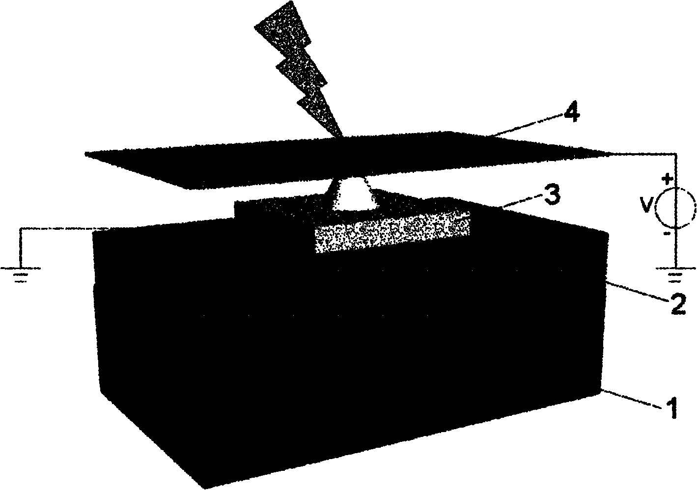
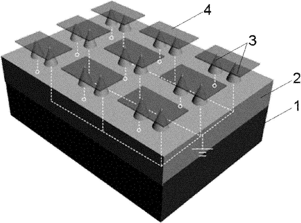
[0020] For the manufacturing process of the point light source array with node single electrode structure, please refer to Figure 4 .

[0021] 1. Chemical vapor deposition (CVD) dielectric layer silicon dioxide;

[0022] 2. The photolithographic dielectric layer, the photolithographic pattern is the pattern of the metal interconnection line inside the dielectric layer;

[0023] 3. Depositing metal interconnection lines: deposit excess metal by evaporation or sputtering, and chemical mechanical polishing (CMP) to smooth the surface;

[0024] 4. Chemical vapor deposition (CVD) dielectric layer silicon dioxide;

[0025] 5. The photolithographic dielectric layer, the photolithographic patterns are metal electrodes and through-hole structures;

[0026] 6. Deposit and polish metal to form electrodes and through-hole structures, the method is the same as 3;

[0027] 7. Etching the dielectric layer, so that the metal electrode has a certain height of protrusion relative to the di...

Embodiment 2

[0033] Specific implementation of node double electrode array structure

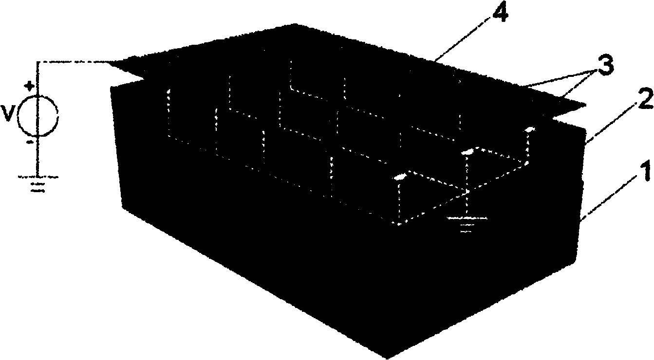
[0034] The manufacturing process flow of the point light source array with the node double electrode structure is similar to that of the previous embodiment, see Figure 4 , after the graphene is transferred to the top of the metal electrode, the graphene etching process is added, and the specific process is as follows:

[0035] 1. Chemical vapor deposition (CVD) dielectric layer silicon dioxide;

[0036] 2. The photolithographic dielectric layer, the photolithographic pattern is the pattern of the metal interconnection line inside the dielectric layer;

[0037] 3. Depositing metal interconnection lines: deposit excess metal by evaporation or sputtering, and chemical mechanical polishing (CMP) to smooth the surface;

[0038] 4. Chemical vapor deposition (CVD) dielectric layer silicon dioxide;

[0039] 5. The photolithographic dielectric layer, the photolithographic patterns are metal electrodes and th...


PUM

PropertyMeasurementUnit
Heightaaaaaaaaaa
Widthaaaaaaaaaa

Abstract

The invention provides an array of graphene-based nano-scale point sources, and belongs to nano-scale luminescent devices. The array of the point sources comprises a substrate, wherein an insulating dielectric layer is covered on the substrate, and a metal interconnecting wire is buried in the dielectric layer; a metal electrode array is arranged above the dielectric layer; the metal interconnecting wire is connected with all electrode in the metal electrode array; and a layer of graphene membrane is coated on the metal electrode array, and a bias voltage is applied on the metal electrodes and the graphene membrane, or a layer of graphene membrane is coated on two adjacent electrodes in the metal electrode array, and a bias voltage is applied between the adjacent electrode pairs. A manufacturing process of the invention can be compatible with the silicon substrate process technology, and has high integrated level; and by the array, the irradiation range and light intensity of light sources can be improved substantially, and the array can be used in high-resolution display devices or information storage systems as a display array or an array of storage units.

Description

technical field [0001] The invention belongs to a nanoscale light emitting device, in particular to an array of graphene-based nanoscale point light sources. Background technique [0002] Currently, nanoscale point light sources are usually based on organic light-emitting diodes or nanowire (tube) structures. Organic light-emitting diodes have been widely used in the display field due to their good spectral regulation and low manufacturing cost. However, the light source structure manufacturing process based on organic light-emitting diodes is poorly compatible with silicon-based semiconductor processes, so its application in the field of nano-optoelectronic devices is greatly limited. With the gradual resolution of the size and doping controllability of the nano light source based on the nanowire structure, it has shown certain application advantages in the field of nanoelectronic devices. In addition, although there are reports of nano light sources based on carbon nanot...

Claims


Application Information

Patent Timeline
IPC IPC(8): H01L27/15
Inventor 王卓邓斯天魏子钧赵华波魏芹芹傅云义黄如张兴
Owner SEMICONDUCTOR MANUFACTURING INTERNATIONAL (BEIJING) CORP
Why Eureka
Try Eureka