Membrane electroluminescent device and preparation method thereof
A technology of electroluminescent devices and thin films, applied in the field of optoelectronics, can solve the problems of insufficient luminous efficiency and achieve the effect of improving electroluminescent efficiency and enhancing luminescence
- Summary
- Abstract
- Description
- Claims
- Application Information
AI Technical Summary
Problems solved by technology
Method used
Image
Examples
preparation example Construction
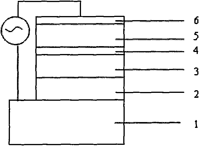
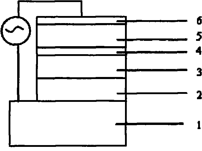
[0029] The present invention also provides a method for preparing the thin film electroluminescent device, which is characterized in that it comprises the following steps:
[0030] S1: preparing a first insulating layer on the ITO conductive glass layer;
[0031] S2: preparing a light-emitting layer on the first insulating layer;
[0032] S3: preparing a metal layer on the light emitting layer;
[0033] S4: preparing a second insulating layer on the metal layer;
[0034] S5: Plating aluminum on the second insulating layer as a metal electrode layer to form a thin film electroluminescent device.
[0035] Wherein, the step S3 further includes: sputtering or evaporating the metal on the surface of the light-emitting layer, and then performing vacuum annealing treatment at 50° C. to 650° C. for 5 minutes to 5 hours, and then naturally cooling to room temperature, thereby A metal layer is prepared on the light emitting layer.
[0036] In the present invention, the preparation m...
Embodiment 1
[0038] Coating SiO on ITO Conductive Glass by Electron Beam Evaporation 2 The thin film is used as a dielectric insulating layer; and then the SiO 2 The surface of the film is coated with a ZnS:Mn light-emitting layer; the surface of the ZnS:Mn light-emitting layer is plated with a silver layer with a thickness of 2nm by magnetron sputtering, and then placed in a vacuum with a degree of better than 1×10 -3 Under the vacuum environment of Pa, after half an hour of annealing treatment at a temperature of 300 ° C, it is cooled to room temperature, and the silver layer forms a non-periodic silver nanoparticle structure layer, that is, a metal layer; Evaporated SiO on the surface 2 thin film as a dielectric insulating layer; finally in SiO 2 A metal Al layer is magnetron sputtered on the surface of the film as an electrode to form a device.
Embodiment 2
[0040] Use magnetron sputtering to coat MgO film on ITO conductive glass as a dielectric insulating layer; then use electron beam evaporation to coat ZnS:Tb, F light-emitting layer on the surface of MgO film, and use magnetron sputtering to coat ZnS: Tb, F luminescent layer coated with a silver layer with a thickness of 4nm, and then put it in a vacuum better than 1×10 -3 Under the vacuum environment of Pa, after annealing at a temperature of 200° C. for forty-five minutes, cool to room temperature, and the silver layer forms a non-periodic silver nanoparticle structure layer, that is, a metal layer; and then magnetron sputtering A MgO thin film is plated on the surface of the metal layer as a dielectric insulating layer, and finally a metal Ag layer is magnetron sputtered on the surface of the MgO thin film as an electrode to form a device.
PUM
| Property | Measurement | Unit |
|---|---|---|
| Thickness | aaaaa | aaaaa |
| Thickness | aaaaa | aaaaa |
Abstract
Description
Claims
Application Information

