Membrane electroluminescent device and preparation method thereof

A technology of electroluminescent devices and thin films, applied in the field of optoelectronics, can solve the problems of insufficient luminous efficiency and achieve the effect of improving electroluminescent efficiency and enhancing luminescence

Inactive Publication Date: 2012-08-01
OCEANS KING LIGHTING SCI&TECH CO LTD
View PDF0 Cites 3 Cited by
  • Summary
  • Abstract
  • Description
  • Claims
  • Application Information

AI Technical Summary

Problems solved by technology

[0004] The technical problem to be solved by the present invention is to provide a thin film electroluminescent device capable of achieving the surface plasmon effect and its preparation method for the defect that the luminous efficiency of the current thin film electroluminescent device is not high enough

Method used


Image

  • Membrane electroluminescent device and preparation method thereof

Examples


preparation example Construction

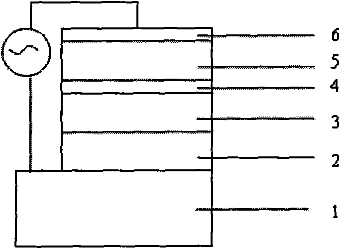
[0029] The present invention also provides a method for preparing the thin film electroluminescent device, which is characterized in that it comprises the following steps:

[0030] S1: preparing a first insulating layer on the ITO conductive glass layer;

[0031] S2: preparing a light-emitting layer on the first insulating layer;

[0032] S3: preparing a metal layer on the light emitting layer;

[0033] S4: preparing a second insulating layer on the metal layer;

[0034] S5: Plating aluminum on the second insulating layer as a metal electrode layer to form a thin film electroluminescent device.

[0035] Wherein, the step S3 further includes: sputtering or evaporating the metal on the surface of the light-emitting layer, and then performing vacuum annealing treatment at 50° C. to 650° C. for 5 minutes to 5 hours, and then naturally cooling to room temperature, thereby A metal layer is prepared on the light emitting layer.

[0036] In the present invention, the preparation m...

Embodiment 1

[0038] Coating SiO on ITO Conductive Glass by Electron Beam Evaporation 2 The thin film is used as a dielectric insulating layer; and then the SiO 2 The surface of the film is coated with a ZnS:Mn light-emitting layer; the surface of the ZnS:Mn light-emitting layer is plated with a silver layer with a thickness of 2nm by magnetron sputtering, and then placed in a vacuum with a degree of better than 1×10 -3 Under the vacuum environment of Pa, after half an hour of annealing treatment at a temperature of 300 ° C, it is cooled to room temperature, and the silver layer forms a non-periodic silver nanoparticle structure layer, that is, a metal layer; Evaporated SiO on the surface 2 thin film as a dielectric insulating layer; finally in SiO 2 A metal Al layer is magnetron sputtered on the surface of the film as an electrode to form a device.

Embodiment 2

[0040] Use magnetron sputtering to coat MgO film on ITO conductive glass as a dielectric insulating layer; then use electron beam evaporation to coat ZnS:Tb, F light-emitting layer on the surface of MgO film, and use magnetron sputtering to coat ZnS: Tb, F luminescent layer coated with a silver layer with a thickness of 4nm, and then put it in a vacuum better than 1×10 -3 Under the vacuum environment of Pa, after annealing at a temperature of 200° C. for forty-five minutes, cool to room temperature, and the silver layer forms a non-periodic silver nanoparticle structure layer, that is, a metal layer; and then magnetron sputtering A MgO thin film is plated on the surface of the metal layer as a dielectric insulating layer, and finally a metal Ag layer is magnetron sputtered on the surface of the MgO thin film as an electrode to form a device.


PUM

PropertyMeasurementUnit
thicknessaaaaaaaaaa
thicknessaaaaaaaaaa
thicknessaaaaaaaaaa

Abstract

The invention relates to a membrane electroluminescent device, which comprises an indium tin oxide (ITO) conducting glass layer, a first insulating layer, a luminescent layer, a second insulating layer and a metal electrode layer which are arranged sequentially, wherein a metal layer with an aperiodic micro-nano structure is arranged between the luminescent layer and the second insulating layer; surface plasma effect can be generated on an interface between the metal layer with the aperiodic micro-nano structure and the luminescent layer; and by the plasma effect, the luminescent effect of the luminescent layer can be enhanced to increase luminescent intensity and improve the electroluminescent efficiency of the device. The invention also provides a preparation method for the membrane electroluminescent device correspondingly.

Description

technical field [0001] The invention relates to the technical field of optoelectronics, and more specifically relates to a thin film electroluminescence device and a preparation method thereof. Background technique [0002] Compared with display devices such as liquid crystal display (LCD), plasma display panel (PDP), light emitting diode (LED), and field emission display (FED), thin film electroluminescent (TFEL) display devices have active luminescence, full solidification, Small size, flat plate, wide viewing angle, wide operating temperature range, high pixel resolution, short response time, anti-vibration and other characteristics, can be applied to the display requirements of various occasions. Traditional thin film electroluminescent devices adopt the MISIM structure (metal-insulating layer-semiconductor light-emitting layer-insulating layer-metal), which is usually deposited on a transparent glass substrate, and metal aluminum and ITO are used as the upper and lower ...

Claims


Application Information

Patent Timeline
Patent Type & Authority Patents(China)
IPC IPC(8): H05B33/14H05B33/10
Inventor 周明杰马文波唐晶
Owner OCEANS KING LIGHTING SCI&TECH CO LTD
Why Eureka
Try Eureka