Method for extracting gate-oxide thickness and substrate doping concentration of field effect transistor

A gate oxide layer thickness, field effect transistor technology, applied in the field of extracting field effect transistor gate oxide layer thickness and substrate doping concentration, can solve the problem of reducing the accuracy of parameters, and achieve the effect of simple structure and high accuracy

Inactive Publication Date: 2011-05-04
PEKING UNIV
View PDF0 Cites 3 Cited by
  • Summary
  • Abstract
  • Description
  • Claims
  • Application Information

AI Technical Summary

Problems solved by technology

Due to the traditional current-voltage or capacitance-voltage characteristics when extracting key parameters of fiel

Method used


Image

  • Method for extracting gate-oxide thickness and substrate doping concentration of field effect transistor
  • Method for extracting gate-oxide thickness and substrate doping concentration of field effect transistor
  • Method for extracting gate-oxide thickness and substrate doping concentration of field effect transistor

Examples


Embodiment 1

[0022] The specific process of using the forward gate-controlled diode to generate-recombined current to extract the gate oxide layer thickness and substrate doping concentration of the SOI field effect transistor is given below:

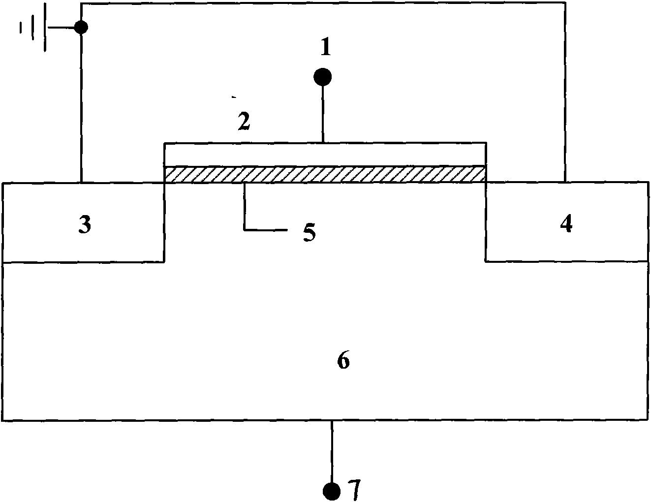
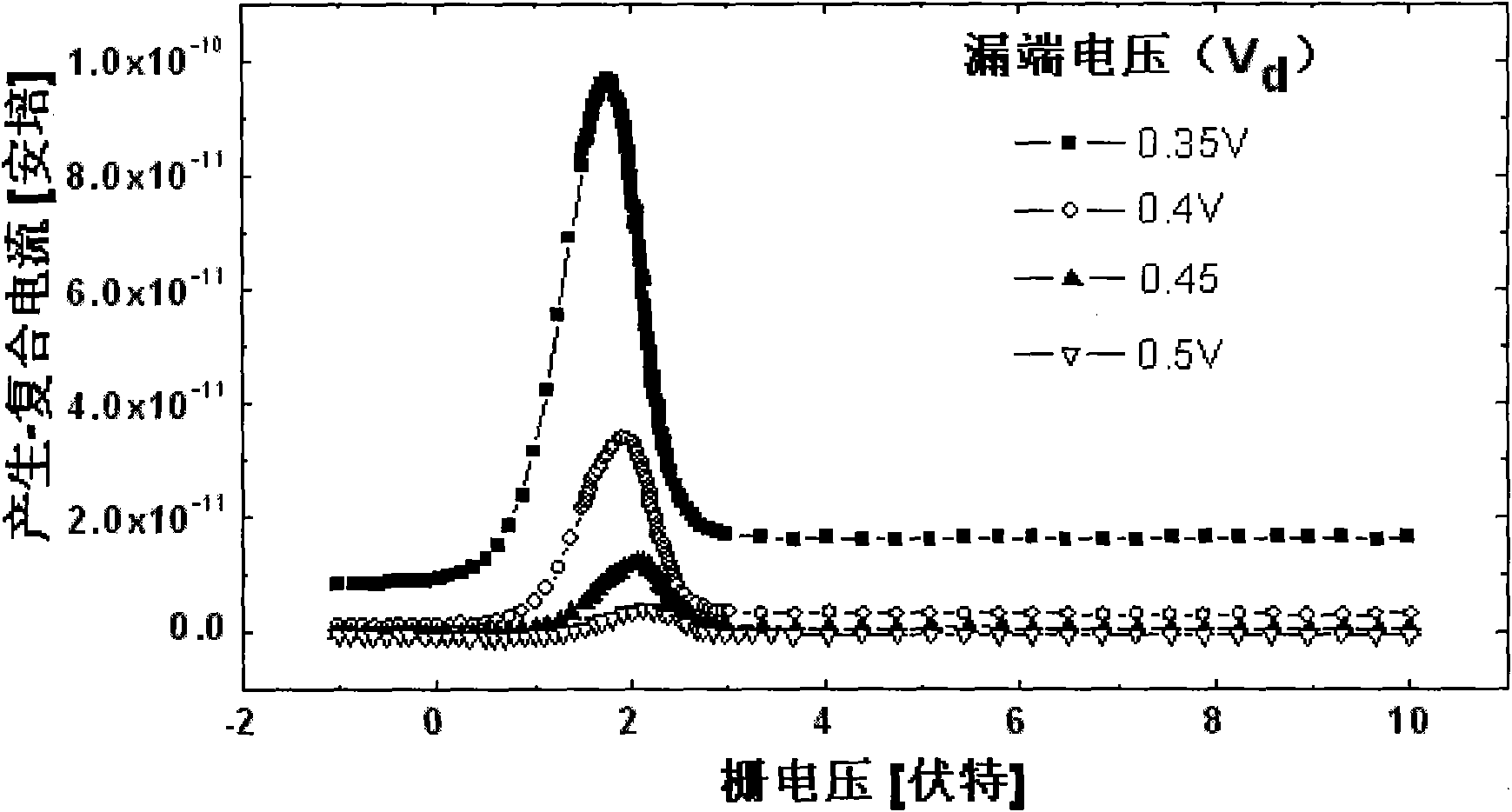
[0023] 1) Ground the source and drain of the SOI field effect transistor, and set the substrate bias voltage to 0.35V, 0.4V, 0.45V and 0.5V respectively, so that the drain-substrate diode is forward biased but not conducting. The test structure diagram is as follows figure 1 Shown; Among them, 1 is the gate voltage, 2 is the gate, 3 is the source, 4 is the drain, 5 is the oxide layer, 6 is the substrate, and 7 is the substrate voltage.

[0024] 2) The gate voltage is swept from -0.5V to +0.5V, and the voltage range includes the gate voltage corresponding to the peak value of the generation-recombination current. Measure the generation-recombination current at the drain, and obtain the relationship curve between generation-recombination current and g...


PUM


Abstract

The invention provides a method for extracting gate oxide thickness and substrate doping concentration of a field effect transistor, which is characterized by comprising the following steps of: grounding a source electrode and a drain electrode of a device, connecting a substrate with smaller positive bias to enable a drain-body diode to be in positive bias and not conducted, scanning gate voltage from negative voltage to a positive voltage, measuring the relation curve of a generation-recombination current of the substrate and the gate voltage, and accurately extracting the gate oxide thickness and the substrate doping concentration of the field effect transistor by utilizing the position shift of the generation-recombination current peak of the positively-biased diode. In the method, a required measuring structure is simple and has high sensitivity and can be used for accurately reflecting the dependence of the gate oxide thickness on the substrate doping concentration.

Description

technical field [0001] The invention belongs to the technical field of integrated circuits and relates to a method for extracting the gate oxide layer thickness and substrate doping concentration of a field effect transistor. Background technique [0002] The increasingly higher integration density and complexity of integrated circuits require a series of requirements for circuit design, such as high precision, short cycle time, low cost, and minimal design errors. As the interface between process and design, the key parameters of semiconductor devices are decisive to ensure the success of integrated circuit design. Because the traditional current-voltage or capacitance-voltage characteristics are easy to be affected by non-ideal factors when extracting key parameters of field effect transistors, the accuracy of parameter extraction is reduced. Contents of the invention [0003] The object of the present invention is to provide a method for extracting the gate oxide layer...

Claims


Application Information

Patent Timeline
IPC IPC(8): G01B7/06G01N27/00
Inventor 马晨月何进张兴
Owner PEKING UNIV
Why Eureka
Try Eureka