Semiconductor device, flip-chip mounting method and flip-chip mounting apparatus

A technology of flip-chip and mounting method, which is applied in the direction of semiconductor devices, semiconductor/solid-state device manufacturing, semiconductor/solid-state device components, etc., and can solve problems such as inability to improve mechanical strength, deviation in shape, and low reliability

Inactive Publication Date: 2011-05-04
PANASONIC CORP
View PDF2 Cites 4 Cited by
  • Summary
  • Abstract
  • Description
  • Claims
  • Application Information

AI Technical Summary

Problems solved by technology

[0009] In the flip-chip mounting method of Patent Document 1, since the process of heating the anisotropic conductive adhesive 52 is controlled so that the unevenness 53 is formed on the chamfer, the unevenness is gentle and the shape varies.
[0010] In addition, in a high-temperature and high-humidity environment, moisture is likely to intrude into the electrical connection between the wiring substrate 50 and the semiconductor chip 51, resulting in low reliability.
[0011] Therefore, while thinking of passing in Figure 46 The container is integrally formed on the component formed in the patent document 2, or a plurality of holes are formed on the surface of the molded resin by using Patent Document 2, and the container is further integrally formed on it, so that a semiconductor with higher mechanical strength and electrical connection reliability can be obtained than before. device, but in any case, it is impossible to form shape-stable unevenness on the surface before forming the container, so the container is easy to come off and the mechanical strength cannot be improved

Method used


Image

  • Semiconductor device, flip-chip mounting method and flip-chip mounting apparatus
  • Semiconductor device, flip-chip mounting method and flip-chip mounting apparatus
  • Semiconductor device, flip-chip mounting method and flip-chip mounting apparatus

Examples


Embodiment approach 1

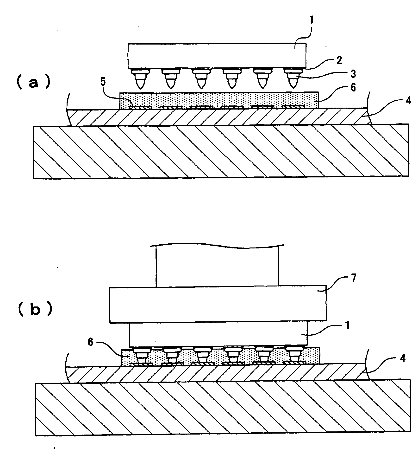
[0075] Figure 1 to Figure 15 Embodiment 1 of this invention is shown.

[0076] Figure 1 to Figure 13 Indicates the process of flip-chip mounting, Figure 13 for the completed semiconductor device.

[0077] First, explain figure 1 (a) The preceding process shown in (b).

[0078] Such as figure 1 As shown in (a), bumps 3 are provided on the electrode pads 2 of the semiconductor chip 1 . The thickness of the semiconductor chip 1 is 0.15 to 0.2 mm. The bump 3 is mainly formed of at least one of gold, copper, palladium, nickel, tin, aluminum, solder, and the like. The bumps 3 may be formed as stud bumps or tear-off bumps by a known wire bonding method, and trace elements may be added or contained in wires for forming the bumps 3 . At this time, the bump height was about 50 μm, and the pedestal diameter was 55 μm. The bump 3 can also be formed by a known plating method or printing method.

[0079] The wiring substrate 4 with a thickness of 0.2 to 0.4mm is a glass epoxy...

Embodiment approach 2

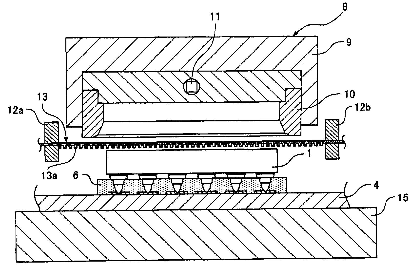
[0106] Figure 16 and Figure 17 Embodiment 2 is shown.

[0107] In Embodiment 1, the film 13 is formed on the surface of the semiconductor chip 1 side. Figure 14 The method of the concave-convex shape 13a of the wavy pattern shown above is different from that of Embodiment 2 only in the following point: the surface of the thin film 13 on the semiconductor chip 1 side is used. Figure 16 The wave-like pattern is shown by the method of the concave-convex shape 13b. Concretely, with regard to the fixed repeating pattern, when the film 13 is manufactured, the concave and convex of the grid-like pattern are formed while performing heat stamping with a roller. Figure 17 The concave-convex part (corrugated part) 16b formed in the chamfer part of the insulating resin 6 is shown. Other parts are the same as Embodiment 1.

Embodiment approach 3

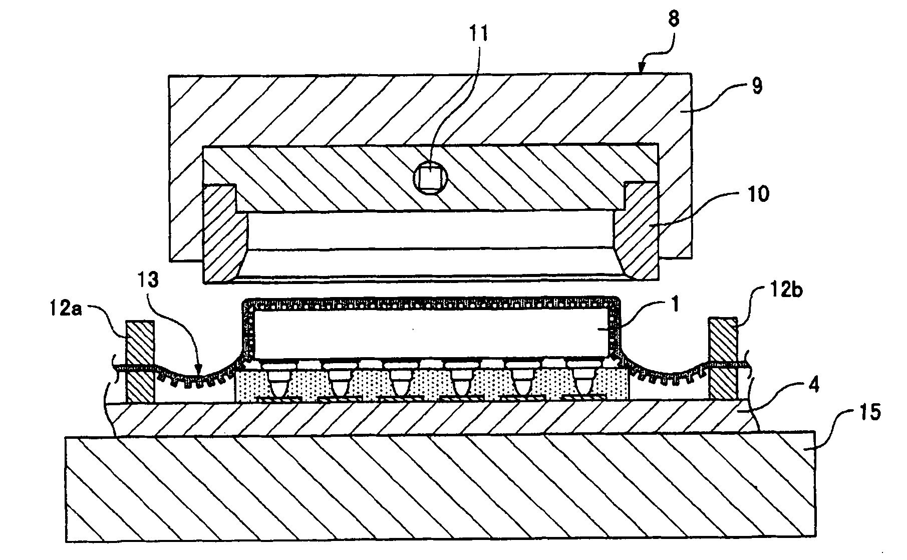
[0109] Figure 18 Embodiment 3 is shown.

[0110] In Embodiment 1 and Embodiment 2, the method of forming the concave-convex shape 13a or 13b on the film 13 is used, and this is transferred to the chamfered portion of the insulating resin 6 to form the concave-convex portion (corrugated portion) 16a or 16b, On the other hand, Embodiment 3 is different only in the following points: the concave-convex portion 10 a is formed on the surface of the frame body 10 of the crimping tool 8 , and the concave-convex portion 10 a is transferred to the chamfered portion of the insulating resin 6 on the surface of the frame body 10 . to form bumps. The finished shape is with Figure 13 same. In the case of Embodiment 3, a thin film having flat surfaces on both sides without forming the concavo-convex shape 13 a on the surface of the thin film 13 on the semiconductor chip 1 side is used.

[0111] In this embodiment using the method of forming the concavo-convex portion 10a on the crimping...


PUM

PropertyMeasurementUnit
Heightaaaaaaaaaa
Diameteraaaaaaaaaa
Thicknessaaaaaaaaaa

Abstract

The invention provides a semiconductor device, a flip-chip mounting method and a flip-chip mounting apparatus. A semiconductor chip (1) is flip-chip mounted on a circuit board (4) with an underfill resin (6) between the semiconductor chip (1) and the circuit board (4). A container covering the semiconductor chip (1) is bonded on the circuit board (4). At this time, the semiconductor chip (1), which is positioned so that the underfill resin (6) is between the circuit board (4) and the semiconductor chip (1), is press heated by a pressure-bonding tool (8). When doing this, the surface of the protruding underfill resin (6) at the periphery of the semiconductor chip (1) is pressed by the pressure-bonding tool (8) through a film (13), which has a periodically repeating pattern of surface relief, so as to form a surface relief (16a). Then, the inner surface of the container covering the semiconductor chip (1) and the surface relief (16a) of the underfill resin surface are bonded to each other.

Description

technical field [0001] The present invention relates to a semiconductor device and a flip chip mounting method. Background technique [0002] In recent years, a semiconductor device in which a bare (bare: bare) semiconductor chip is directly mounted on a wiring board (bare chip mounting) has been demanded due to demands for smaller and thinner electronic equipment. In particular, there is a demand for a semiconductor device in which a circuit surface of a semiconductor chip is mounted upside down (flip chip mounting) on ​​a wiring board so as to face it. [0003] Conventionally, flip-chip semiconductor devices such as Figure 45 As shown, a semiconductor chip 51 including internal connection terminals such as metal bump electrodes is mounted on a wiring substrate 50 by flip-chip connection. 52 is an anisotropic conductive adhesive. [0004] In this semiconductor device, when an external force acts on the semiconductor chip 51 , the anisotropic conductive adhesive 52 is dam...

Claims


Application Information

Patent Timeline
IPC IPC(8): H01L21/60H01L21/56
CPCH01L21/563H01L21/565H01L21/568H01L23/3121H01L23/3142H01L24/16H01L24/32H01L24/75H01L24/81H01L24/83H01L2224/1134H01L2224/13124H01L2224/13144H01L2224/13147H01L2224/13155H01L2224/13164H01L2224/16225H01L2224/2919H01L2224/32H01L2224/32225H01L2224/48227H01L2224/73204H01L2224/75H01L2224/75303H01L2224/75313H01L2224/75315H01L2224/75317H01L2224/75501H01L2224/81001H01L2224/81005H01L2224/81191H01L2224/81203H01L2224/81801H01L2224/83192H01L2224/83203H01L2224/83856H01L2224/9221H01L2924/01004H01L2924/01005H01L2924/01006H01L2924/01013H01L2924/01029H01L2924/01033H01L2924/01046H01L2924/0105H01L2924/01058H01L2924/01078H01L2924/01079H01L2924/01082H01L2924/014H01L2924/0665H01L2924/07811H01L2924/181H01L2924/3025H01L2924/00H01L2924/3512
Inventor 户村善广清水一路熊泽谦太郎
Owner PANASONIC CORP
Why Eureka
Try Eureka