Supercharge Your Innovation With Domain-Expert AI Agents!

Cell structure of one-time programmable memory (OTP) device and manufacturing method and operating method of cell structure

A technology of unit structure and manufacturing method, which is applied in semiconductor/solid-state device manufacturing, electric solid-state devices, semiconductor devices, etc., can solve the problems of unfavorable high-density integrated circuit application and large unit structure area, and achieve reliable data storage capacity, small area effect

Active Publication Date: 2011-05-18
SHANGHAI HUAHONG GRACE SEMICON MFG CORP
View PDF7 Cites 7 Cited by
  • Summary
  • Abstract
  • Description
  • Claims
  • Application Information

AI Technical Summary

Problems solved by technology

Due to the existence of the floating gate coupling capacitor 1a, the unit structure area of ​​this OTP device is too large, which is not conducive to the application of high-density integrated circuits

Method used


Image

  • Cell structure of one-time programmable memory (OTP) device and manufacturing method and operating method of cell structure
  • Cell structure of one-time programmable memory (OTP) device and manufacturing method and operating method of cell structure
  • Cell structure of one-time programmable memory (OTP) device and manufacturing method and operating method of cell structure

Examples


Embodiment Construction

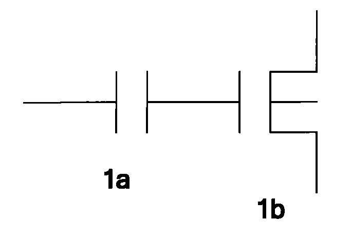
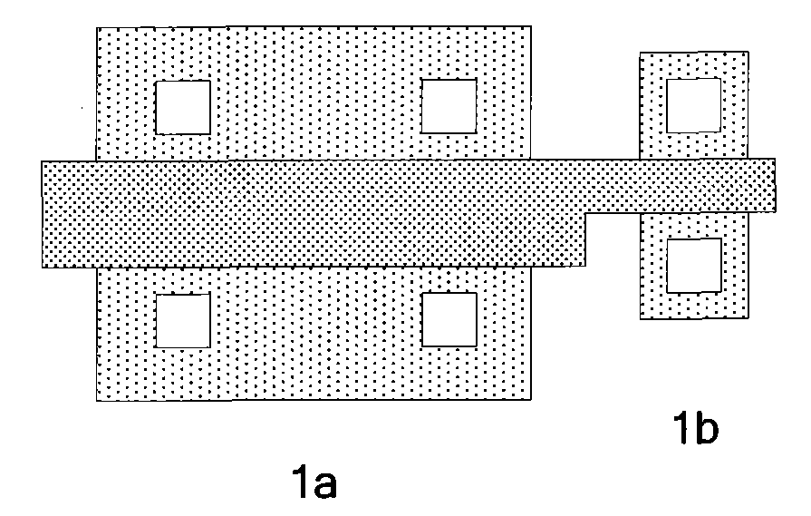
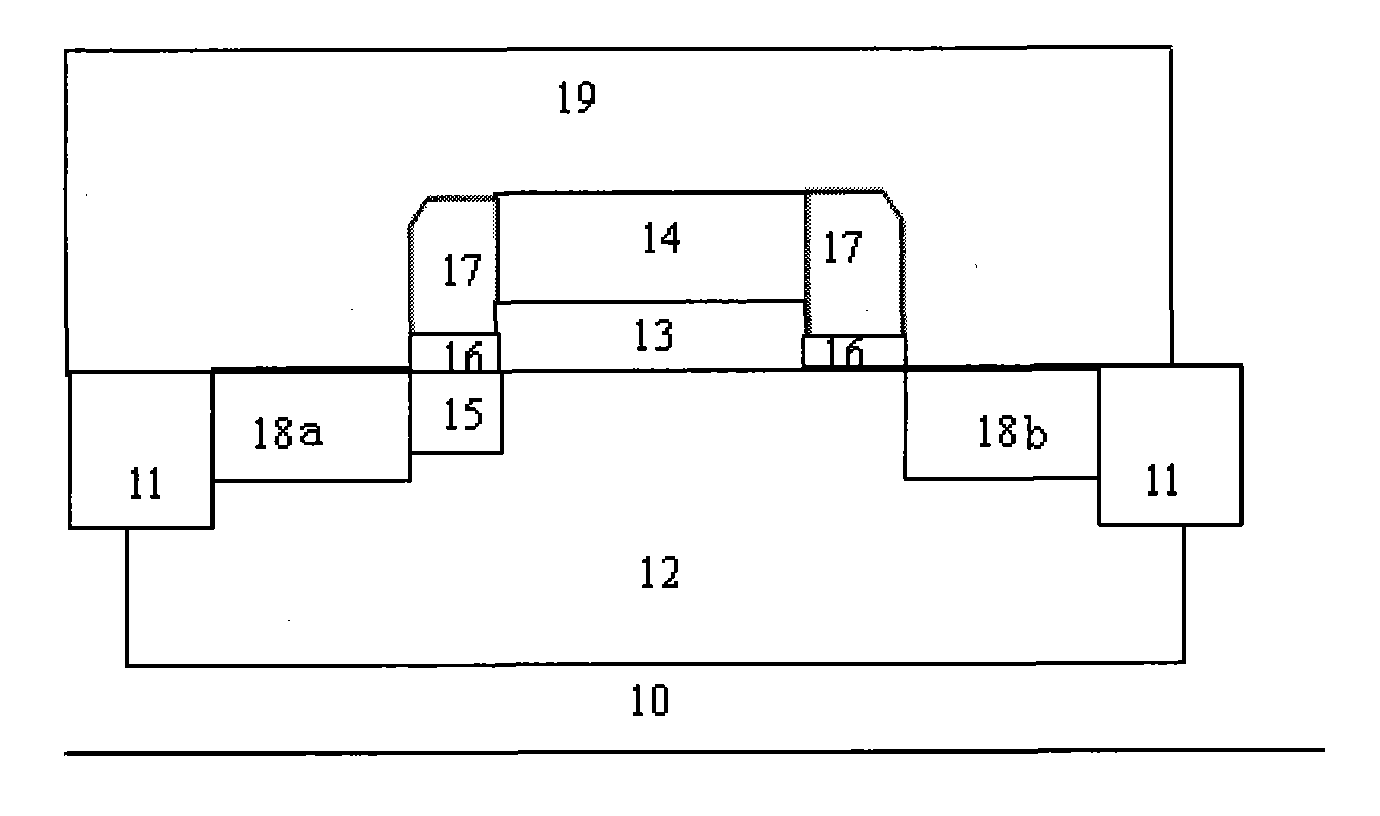
[0032] see figure 2 , the unit structure of the OTP device of the present invention is an NMOS, and a p-well 12 is formed on the substrate 10 . There is an isolation region 11 in the substrate 10 and / or the p-well 12, which is generally made of dielectric materials such as silicon dioxide, silicon nitride, silicon oxynitride and the like. On the p-well 12 there is a gate oxide layer 13 and silicon dioxide 16 , and the silicon dioxide 16 is on both sides of the gate oxide layer 13 . On the gate oxide layer 13 is a polysilicon gate 14 , on the silicon dioxide 16 there are silicon nitride sidewalls 17 , and the silicon nitride sidewalls 17 are on both sides of the polysilicon gate 14 . The polysilicon gate 14 only has an n-type lightly doped region 15 in the p-well 12 under one side. There are n-type heavily doped regions 18a and 18b in the p well 12 below the outer side of the silicon nitride spacer wall 17 . The surface of the silicon wafer is covered with a layer of silico...


PUM


Abstract

The invention discloses a cell structure of a one-time programmable memory (OTP) device. The cell structure is characterized in that silicon dioxides (16) are arranged at the two sides of a gate oxide (13); silicon nitride side walls (17) are arranged on the silicon dioxides (16); and a lightly doped region (15) is arranged below only one side of a polysilicon gate (14). By removing the lightly doped region (15) at the other side, the generation probability and quantity of hot electrons are improved and the hot electrons penetrate through the barriers of the silicon dioxides (16) and are captured by the silicon nitride side walls (17), thus implementing programming by using a channel hot electron injection (CHE) mechanism. In the cell structure, the polysilicon gate (14) is used as a wordline, an n-type heavily doped region (18a) adjacent to the n-type lightly doped region (15) is used as a bit line; and an n-type heavily doped region (18b) not adjacent to the n-type lightly doped region (15) is used as the programming terminal. The invention also discloses a manufacturing method and an operating method of the cell structure of the OTP device. The cell structure has small area and is applicable to the condition of thinner gate oxide.

Description

technical field [0001] The invention relates to an OTP (one-time programmable memory, one-time programmable memory) device, in particular to a unit structure of the OTP device. Background technique [0002] There are currently two representative types of unit structures for OTP devices. [0003] see Figure 1a , Figure 1b , the unit structure of the first type of OTP device consists of a transistor 1b and a floating gate capacitor 1a, where the transistor 1b performs the programming function, the floating gate capacitor 1a performs the charge storage function, and the polysilicon gate of the transistor 1b extends to the floating gate capacitor 1a. Above, the floating gate capacitor 1a is a plate capacitor formed by the extended polysilicon and the silicon below it. Chinese Invention Patent Application Publication CN1627525A (published on June 15, 2005) and Chinese Invention Patent Application Publication CN1627526A (published on June 15, 2005) both disclose the unit struc...

Claims


Application Information

Patent Timeline
Patent Type & Authority Applications(China)
IPC IPC(8): H01L27/115H01L21/8247G11C17/08H10B69/00
Inventor 胡晓明
Owner SHANGHAI HUAHONG GRACE SEMICON MFG CORP
Features
  • R&D
  • Intellectual Property
  • Life Sciences
  • Materials
  • Tech Scout
  • Unparalleled Data Quality
  • Higher Quality Content
  • 60% Fewer Hallucinations
Learn More