
Movable structure and optical scanning mirror using same

A structure and moving plate technology, applied in the direction of microstructure technology, microstructure devices composed of deformable elements, microstructure devices, etc. Impact enhancement effect

Inactive Publication Date: 2011-05-18
PANASONIC CORP
View PDF14 Cites 12 Cited by
  • Summary
  • Abstract
  • Description
  • Claims
  • Application Information

AI Technical Summary

Problems solved by technology

Since each comb is thin and fragile, there is a possibility of breakage when it comes into contact with a fixed frame or a movable plate like this

Method used


Image

  • Movable structure and optical scanning mirror using same
  • Movable structure and optical scanning mirror using same
  • Movable structure and optical scanning mirror using same

Examples


no. 1 approach

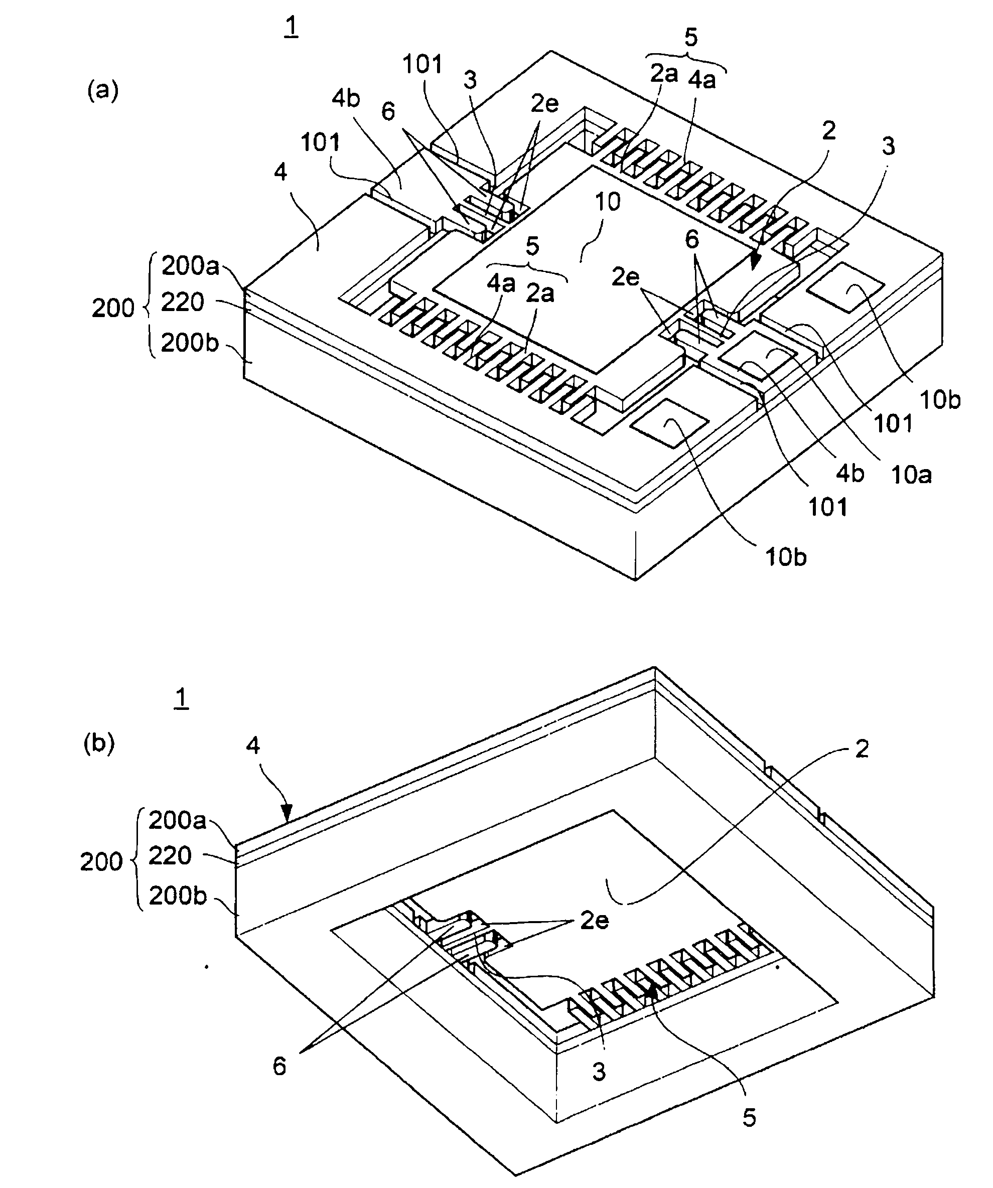
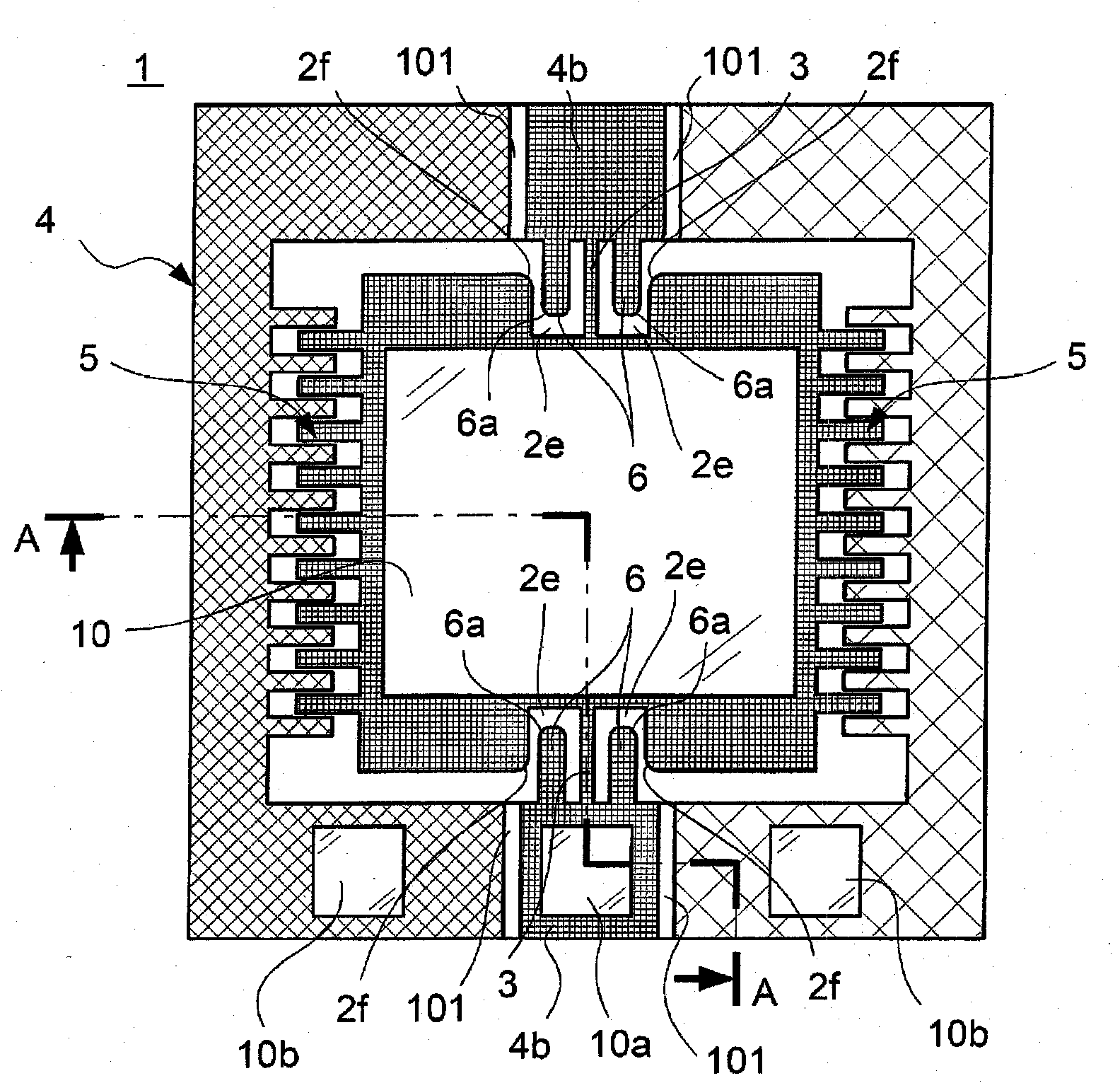
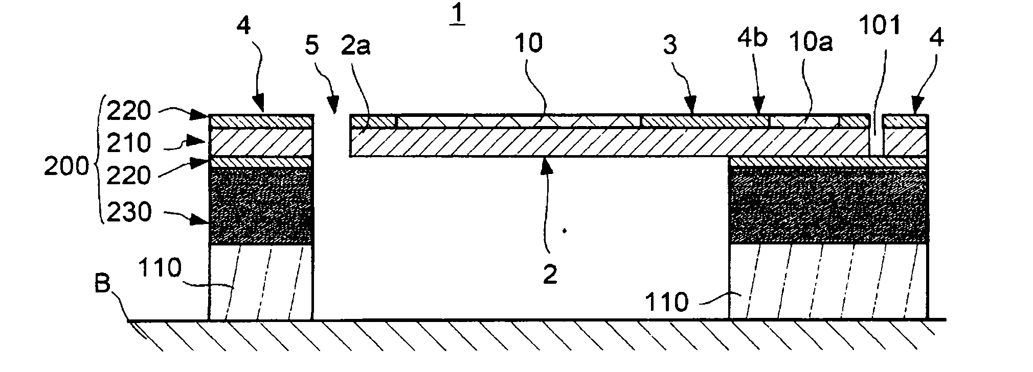
[0066] Next, a first embodiment of the present invention will be described with reference to the drawings. figure 1 (a), (b), figure 2 and image 3 An example of the optical scanning mirror (movable structure) of this embodiment is shown. The optical scanning mirror 1 is, for example, a small member mounted on a barcode reader, a projector device that projects an image on an external screen, or an optical device such as an optical switch, and has a scanning function incident from an external light source or the like (not shown). The function of the beam, etc.

[0067] First, the configuration of the optical scanning mirror 1 will be described below. The optical scanning mirror 1 is a MEMS (Micro Electro Mechanical System) element manufactured by processing an SOI (Silicon on Insulator) substrate 200 using a so-called micromachining technique or the like. The SOI substrate 200 is formed by, for example, bonding a conductive first silicon layer (active layer) 200a and a sec...

no. 2 approach

[0083] Next, a second embodiment of the present invention will be described. Figure 5 The light scanning mirror 21 of the second embodiment is shown. Hereinafter, the same reference numerals are used for the same components as those of the above-mentioned first embodiment, and only the parts that are different from the above-mentioned first embodiment will be described. The light scanning mirror 21 has a movable plate 22 having a different shape from the movable plate 2 of the light scanning mirror 1 . That is, as shown in the drawing, the movable plate 22 does not have the concave portion 2e, and has stoppers formed to protrude toward the fixed frame 4 at positions farther from the hinge 3 than the stopper portion 6 on both side portions of the hinge 3 . contact protrusion 22e. Other configurations of the movable plate 22 and configurations other than the movable plate 22 of the light scanning mirror 21 are the same as those of the light scanning mirror 1 according to the ...

no. 3 approach

[0086] Figure 7 A light scanning mirror 41 according to a third embodiment of the present invention is shown. The optical scanning mirror 41 includes a movable plate 42 having a stopper portion 46 formed along the hinge 3 instead of the movable plate 2 of the optical scanning mirror 1 . In addition, in the support portion 4b of the fixed frame 4, a contact protrusion 44e is provided. The abutment protrusions 44 e are formed to protrude toward the movable plate 42 at positions farther from the hinge 3 than the stopper portion 46 on both side portions of the hinge 3 . The configuration of the optical scanning mirror 41 other than the movable plate 42 and the contact protrusion 44e is the same as that of the optical scanning mirror 1 of the first embodiment. The optical scanning mirror 41 is also formed into a shape including the movable plate 42 and the contact protrusion 44e by processing the first silicon layer 200a by bulk micromachining technology, and can be easily manuf...


PUM


Abstract

An impact resistance is enhanced by preventing hinges from being damaged even if an impact is provided from the outside thereto in a semiconductor machine structure. An optical scanning mirror (1) comprises a movable plate (2), the pair of hinges (3) which have one ends connected to both sides of the movable plate (2), respectively, and which form one swing axis of the movable plate (2), a fixed frame (4) so disposed as to surround the movable plate (2) and supporting the other ends of the hinges (3), and stopper parts (6) formed on the fixed frame (4). When the movable plate (2) is displaced sideways, the stopper parts (6) are brought into contact with the side edges of the recesses (2e) of the movable plate (2), and the displacement of the movable plate (2) sideways is restricted. Consequently, the hinges (3) are prevented from being damaged even if an impact is provided from the outside thereto.

Description

technical field [0001] The present invention relates to a movable structure formed on a semiconductor substrate and having a movable plate pivotally supported by a hinge and configured to be swingable. Background technique [0002] Conventionally, for example, as an optical device such as a barcode reader or a projector, there is known a device using an optical scanning mirror that swings a movable plate provided with a mirror surface, and responds to a light beam incident on the mirror surface, etc. Scanning is performed (for example, refer to Patent Document 1 to Patent Document 3). As an optical scanning mirror, for example, a small optical scanning mirror having a semiconductor movable structure formed using a micromachining technique is known. Such a movable structure has a movable plate that forms a mirror surface when used as an optical scanning mirror, and a fixed frame that supports the movable plate. The movable plate and the fixed frame are connected by hinges. ...

Claims


Application Information

Patent Timeline
Patent Type & Authority Applications(China)
IPC IPC(8): H02N1/00B81B3/00G02B26/08G02B26/10
CPCB81B3/0051B81C2203/031H02N1/006G02B26/0841B81C2203/0118B81C2201/112B81B2201/042Y10T403/32557
Inventor 橘宏明野毛宏河野清彦上田英喜
Owner PANASONIC CORP
Learn More