Chip for measuring ohmic contact degradation of semiconductor device and method

An ohmic contact and semiconductor technology, used in semiconductor devices, single semiconductor device testing, semiconductor/solid-state device manufacturing, etc., can solve the problems of inability to assess the degradation of ohmic contact resistance, loss of semiconductor materials, and inability to directly apply assessment current to achieve accurate Effective ohmic contact, accurate and effective evaluation, and the effect of meeting the requirements of high current impact

Inactive Publication Date: 2011-05-25
BEIJING UNIV OF TECH
View PDF2 Cites 8 Cited by
  • Summary
  • Abstract
  • Description
  • Claims
  • Application Information

AI Technical Summary

Problems solved by technology

However, when it is necessary to detect ohmic contact resistivity at high current densities (×10 3-5 A / cm 2 ) in the use environment, when the ohmic contact resistivity degrades or fails, the structure cannot directly apply the test current
If a current is directly applied between the electrodes, the degradation of the ohmic contact resistance will also cause loss of the semiconductor material between the two contact rings, so that the measured ohmic contact degradation also includes the degradation of the semiconductor material, which cannot truly reflect Degradation of Ohmic Contact
That is, the structure and method of the ohmic contact measuring chip in the prior art can only measure the degradation of the ohmic contact resistivity, but cannot assess the degradation of the ohmic contact resistance with the operating current

Method used


Image

  • Chip for measuring ohmic contact degradation of semiconductor device and method
  • Chip for measuring ohmic contact degradation of semiconductor device and method
  • Chip for measuring ohmic contact degradation of semiconductor device and method

Examples


Embodiment Construction

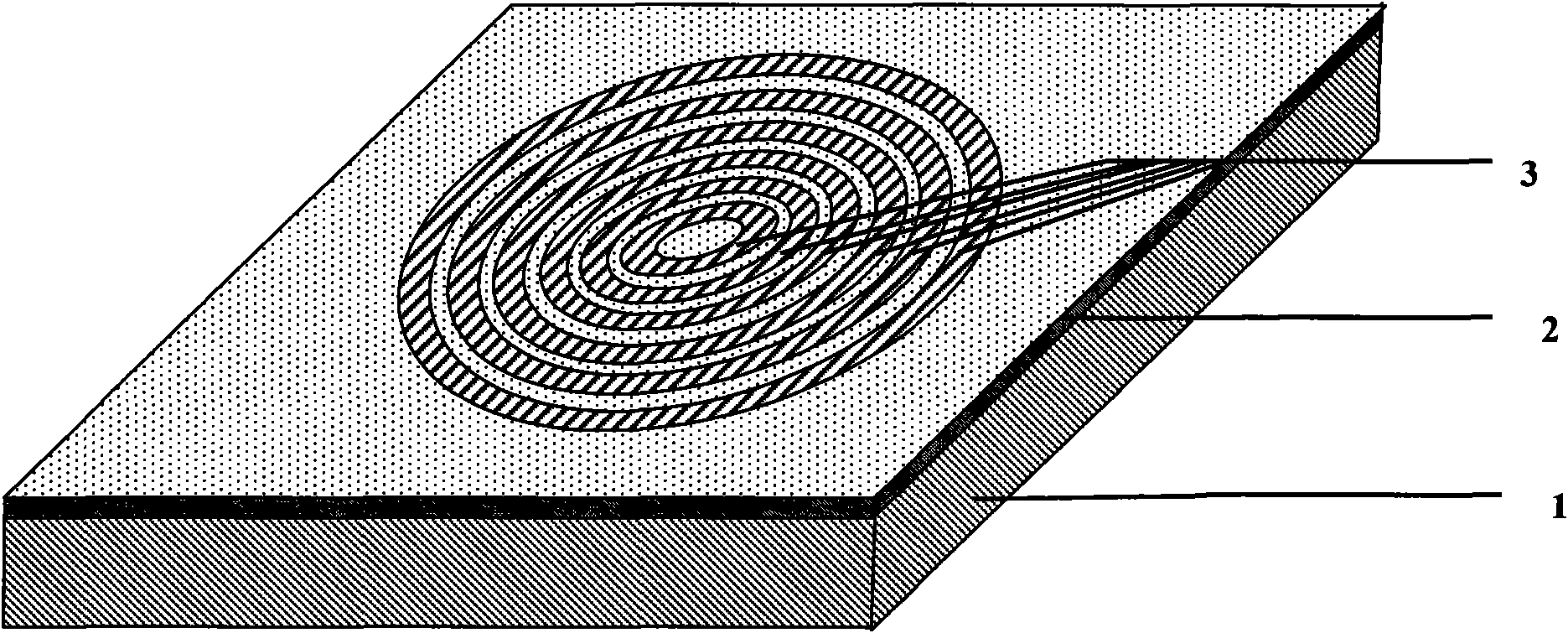
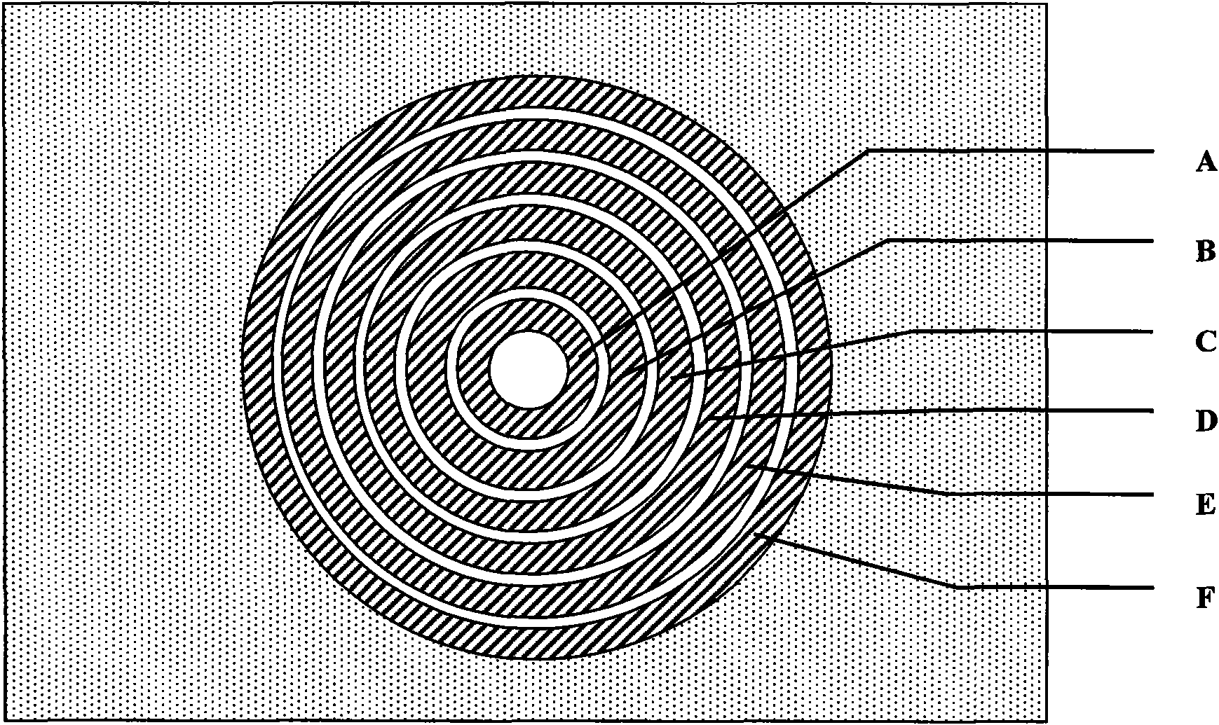
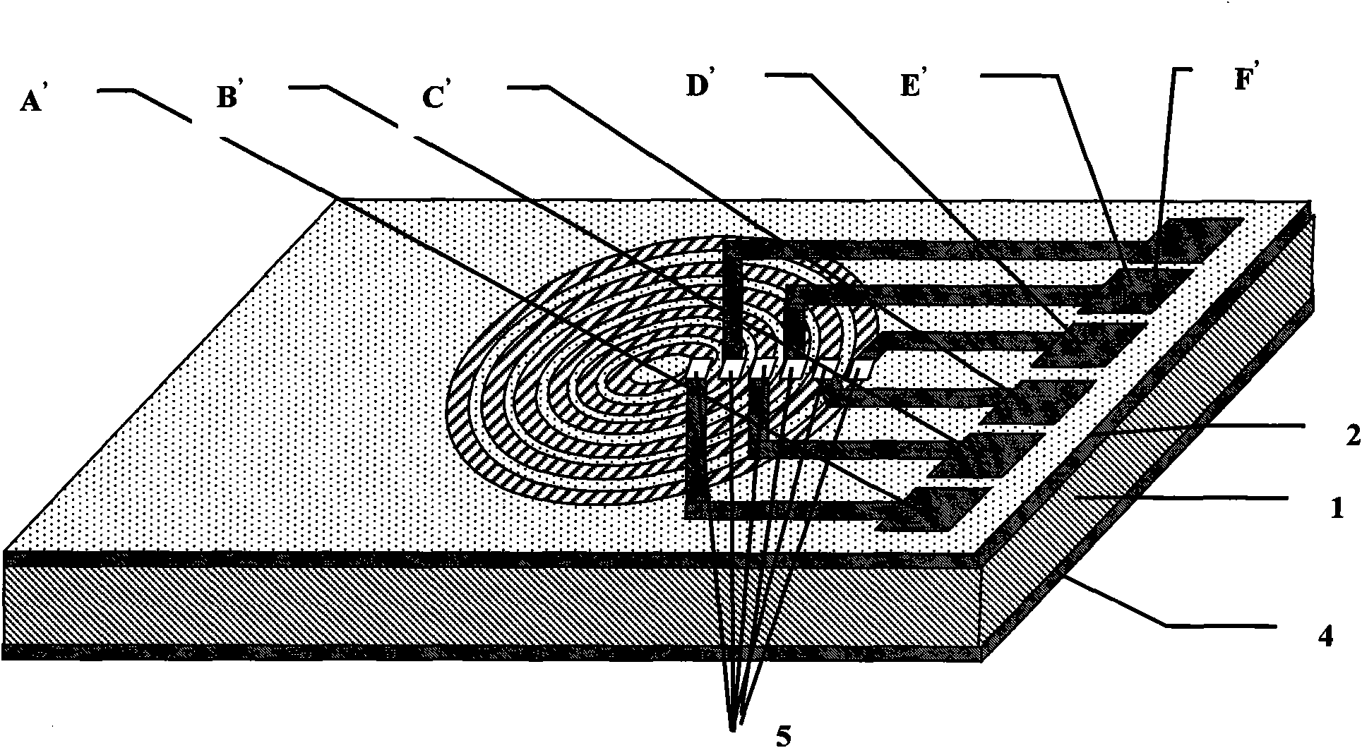
[0027] See image 3 The chip for measuring the ohmic contact degradation failure of semiconductor devices used to achieve the purpose of the present invention includes preparing a semiconductor epitaxial material 2 on a semiconductor wafer substrate 1, and the thickness of the semiconductor wafer substrate is 50 μm. Using a specific ohmic contact process, prepare the ring electrode 3 fixed to the surface of the semiconductor epitaxial material 2, the electrode 3 includes 6 ring electrodes (A, B, C, D, E, F), and prepare the back electrode on the back of the substrate 1 4. A layer of insulating dielectric film is deposited on the surface of the prepared chip, and external electrode windows are carved on the ring electrodes (A, B, C, D, E, F) by photolithography technology, and these windows are arranged in a straight line. And contact electrodes A', B', C', D', E', F' with large external areas. Generally, the thickness of the prepared ohmic contact semiconductor epitaxial mat...


PUM


Abstract

The invention provides a chip for measuring ohmic contact degradation of a semiconductor device and a method, belonging to semiconductor technology, especially the field of failure evaluation of semiconductor devices. The invention provides the chip special for measuring ohmic contact degradation. The chip is characterized in that an SiO2 insulating medium layer is deposited on the circle ohmic contact surface of a circle transmission line method (CTLM) ohmic contact testing chip with at least 6 circle electrodes, a back electrode prepared by a metal deposition process is arranged on the other surface of the CTLM ohmic contact testing chip and then an outer electrode is fixedly connected on each circle electrode; and the fixed connection points of the circle electrodes and the outer electrodes are arranged on one straight line. Not only can the change relationship of the ohmic contact resistivity of the semiconductor chip along with the applied current and the relationship of the ohmic contact resistivity along with the current applying time be measured by adopting the chip and the method, but also the chip can meet the requirement of large current shock. Therefore, ohmic contact can be evaluated more accurately and effectively by using the chip and method provided by the invention.

Description

technical field [0001] The invention belongs to semiconductor technology, especially the field of failure evaluation of semiconductor devices. Background technique [0002] The ohmic contact in semiconductor technology refers to the area where the metal lead and the semiconductor contact on the semiconductor device. Any semiconductor device needs to have good ohmic contact characteristics, that is, it requires a very good linear contact between the semiconductor and the metal, small additional resistance, and good long-term use stability. The ohmic contact will degrade after high current and long-term use, that is, the resistance becomes larger, the linearity changes and the stability becomes worse. [0003] In order to make the chip still have good ohmic contact performance under high current density, it is necessary to accurately measure the degradation of chip ohmic contact resistance under high current. The measurement of ohmic contact resistance usually adopts transmi...

Claims


Application Information

Patent Timeline
Patent Type & Authority Applications(China)
IPC IPC(8): H01L23/544G01R31/26H01L21/02
Inventor 冯士维乔彦彬郭春生张光沉邓海涛
Owner BEIJING UNIV OF TECH
Why Eureka
Try Eureka