Chemical vapor deposition method assisted by non-plasma

A chemical vapor deposition, non-plasma technology, applied in gaseous chemical plating, metal material coating process, coating, etc., can solve problems affecting chip quality, large error range, etc., to reduce the range of changes and reduce changes range effect

Active Publication Date: 2013-09-18
SEMICON MFG INT (SHANGHAI) CORP +1
View PDF0 Cites 0 Cited by
  • Summary
  • Abstract
  • Description
  • Claims
  • Application Information

AI Technical Summary

Problems solved by technology

Since the thickness of the dielectric layer produced on the non-plasma-assisted chemical vapor deposition reaction chamber wafer is different, and the resistance of the through hole is proportional to the thickness of the dielectric layer, this makes the error range of the contact resistance of the chip produced on the wafer Larger, affecting the quality of the chip

Method used


Image

  • Chemical vapor deposition method assisted by non-plasma
  • Chemical vapor deposition method assisted by non-plasma

Examples


Embodiment Construction

[0026] In order to make the object, technical solution, and advantages of the present invention clearer, the present invention will be further described in detail below with reference to the accompanying drawings and examples.

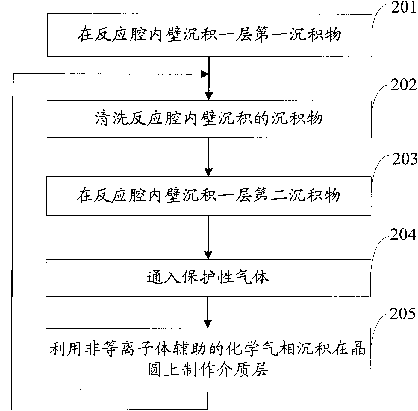
[0027] The present invention proposes a non-plasma-assisted chemical vapor deposition method. In the method, before the wafer is placed in the reaction chamber, the deposit deposited on the inner wall of the reaction chamber is cleaned, and a layer of second deposition is deposited on the inner wall of the reaction chamber. According to the air pressure in the reaction chamber, the time for feeding the protective gas is adjusted; after the wafer is placed in the reaction chamber, a dielectric layer is made on the wafer by non-plasma-assisted chemical vapor deposition.

[0028] figure 2 It is a flow chart of the non-plasma-assisted chemical vapor deposition method of the present invention. Combine now figure 2 , the method for non-plasma-assisted ch...


PUM

PropertyMeasurementUnit
thicknessaaaaaaaaaa

Abstract

The invention provides a chemical vapor deposition method assisted by non-plasma. The method comprises the following steps: cleaning sediment deposited on the inner wall of a reaction cavity before placing a wafer in the reaction cavity, depositing a layer of second sediment on the inner wall of the reaction cavity, and regulating the time of introducing protective gas according to the air pressure in the reaction cavity; and after placing the wafer in the reaction cavity, preparing a dielectric layer on the wafer by using the chemical vapor deposition method assisted by the non-plasma. By using the method, the sediment deposited on the inner wall of the reaction cavity is cleaned before placing the wafer in the reaction cavity so as to clean the sediment remained on the inner wall of the reaction cavity, then a layer of second sediment is deposited on the inner wall of the reaction cavity so that the environments in the reaction cavity are consistent with the environment when the wafer is placed in the reaction cavity to manufacture the dielectric layer; and through cleaning the reaction cavity and regulating the introduction time of the protective gas, the severe variation of the temperature in the reaction cavity is avoided so as to influence the thickness of the sequentially manufactured dielectric layer, and the variation range of the thickness of the dielectric layer is reduced.

Description

technical field [0001] The invention relates to semiconductor manufacturing technology, in particular to a non-plasma assisted chemical vapor deposition method. Background technique [0002] In the semiconductor manufacturing process, several active devices are usually fabricated on the wafer, and the dielectric layer and the metal layer are fabricated layer by layer on the active device through the deposition process, through the dielectric layer, the through hole opened in the dielectric layer, through the The different metal layers connected by the holes connect the active devices fabricated on the wafer, which is the process of multi-layer metallization of the wafer. The interconnects formed on the metal layer are connected through the vias formed on the insulating layer to connect the active devices on the wafer. [0003] figure 1 It is a structural schematic diagram of multi-layer metallization on an existing wafer. Combine now figure 1 , the method of chemical vap...

Claims


Application Information

Patent Timeline
Patent Type & Authority Patents(China)
IPC IPC(8): C23C16/455C23C16/52
Inventor 徐强
Owner SEMICON MFG INT (SHANGHAI) CORP
Why Eureka
Try Eureka