Laser processing device

A laser processing and laser technology, applied in auxiliary devices, metal processing, laser welding equipment, etc., can solve unsolvable problems

Active Publication Date: 2011-06-15
DISCO CORP
View PDF8 Cites 23 Cited by
  • Summary
  • Abstract
  • Description
  • Claims
  • Application Information

AI Technical Summary

Problems solved by technology

[0008] However, even in the laser processing device equipped with the dust discharge member described in the above-mentioned Patent Document 2, it cannot be solved that the dust s

Method used


Image

  • Laser processing device
  • Laser processing device
  • Laser processing device

Examples


Embodiment Construction

[0025] Hereinafter, preferred embodiments of the laser processing apparatus configured according to the present invention will be described in more detail with reference to the drawings.

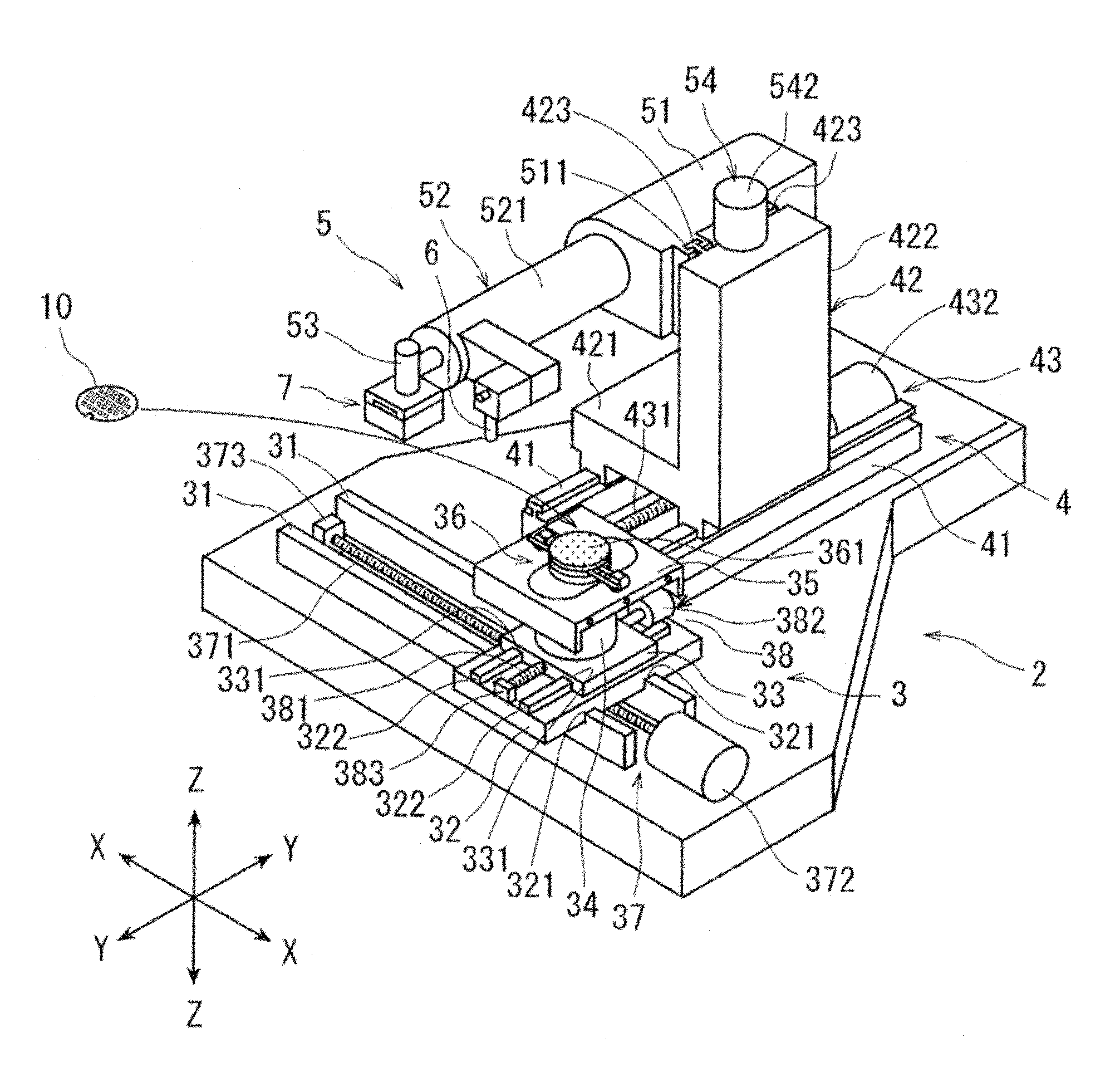
[0026] exist figure 1 A perspective view of a laser processing device constructed according to the present invention is shown in . figure 1 The shown laser processing device is equipped with: a stationary base 2; a chuck table mechanism 3, which is arranged on the stationary base 2 in a manner capable of moving along the processing feed direction shown by the arrow X, and is used to hold the workpiece to be processed. object; a laser light irradiation unit support mechanism 4, which is arranged on the stationary base 2 in a manner capable of moving along the indexing feed direction shown by the arrow Y that is at right angles to the direction shown by the above arrow X; and laser light irradiation The unit 5 is disposed on the laser beam irradiation unit support mechanism 4 so as to be mova...


PUM


Abstract

The invention provides a laser processing device, which is capable of effectively collecting and discharging dust like debris generated by irradiating laser ray from a condenser to an object to be processed. The laser ray irradiation component comprises a laser ray oscillator, a condenser having a condensing lens for condensing laser rays, and a dust discharging component which is disposed at the end of the condenser near the downstream side of the laser ray irradiation direction. The dust discharging component comprises a dust collector, consisting of an upstream sidewall, a downstream sidewall and an outer sidewall. The upstream sidewall is provided with a first opening which enables the laser ray irradiated from the condenser to pass and acquire air obtain. The downstream sidewall is provided with a second opening which enables the laser ray irradiated through the first opening to pass and suck dust. The outer sidewall is connected to the upstream sidewall and the downstream sidewall, forming a dust collecting room. The outer sidewall is provided with an exhaust outlet enabling the dust collecting room and a suction source to commutate with each other. An outer air acquiring channel which enables the first opening to communicated with the outer air is disposed between the dust collector and the condenser.

Description

technical field [0001] The present invention relates to a laser processing device for performing laser processing on a workpiece such as a semiconductor wafer. Background technique [0002] In the manufacturing process of a semiconductor device, a plurality of regions are divided on the surface of a roughly disc-shaped semiconductor wafer by dividing lines called streets arranged in a grid pattern, and ICs are formed in the divided regions ( Integrated Circuit: integrated circuit), LSI (large scale integration: large scale integrated circuit) and other devices. Then, by cutting the semiconductor wafer along the lanes, the regions where the devices are formed are divided to manufacture individual devices. In addition, for an optical device wafer formed by stacking light-receiving elements such as light-emitting diodes or light-emitting elements such as laser diodes on the surface of a sapphire substrate, it is also divided into individual optical devices such as light-emitti...

Claims


Application Information

Patent Timeline
IPC IPC(8): B23K26/00B23K26/16B23K26/142
CPCB23K26/064B23K26/142B23K26/16B23K26/706B23K37/0461B23K2101/40
Inventor 小田中健太郎大庭龙吾
Owner DISCO CORP
Why Eureka
Try Eureka