Manufacturing method of high-K metal gate MOS (Metal Oxide Semiconductor) transistor

A MOS transistor and metal gate technology, which is applied in the field of manufacturing high-K metal gate MOS transistors, can solve the problems of reduced transistor driving capability, increased parasitic resistance of source and drain regions, etc. Effect

Active Publication Date: 2011-06-29
PEKING UNIV SHENZHEN GRADUATE SCHOOL
View PDF7 Cites 2 Cited by
  • Summary
  • Abstract
  • Description
  • Claims
  • Application Information

AI Technical Summary

Problems solved by technology

However, such doping will form a serious impurity compensation effect in the source and drain regions, resulting in an increase in the parasitic resistance of the source and drain regions and a decrease in the driving capability of the transistor.

Method used


Image

  • Manufacturing method of high-K metal gate MOS (Metal Oxide Semiconductor) transistor
  • Manufacturing method of high-K metal gate MOS (Metal Oxide Semiconductor) transistor
  • Manufacturing method of high-K metal gate MOS (Metal Oxide Semiconductor) transistor

Examples


Embodiment Construction

[0029] The present invention will be further described in detail below through specific embodiments in conjunction with the accompanying drawings.

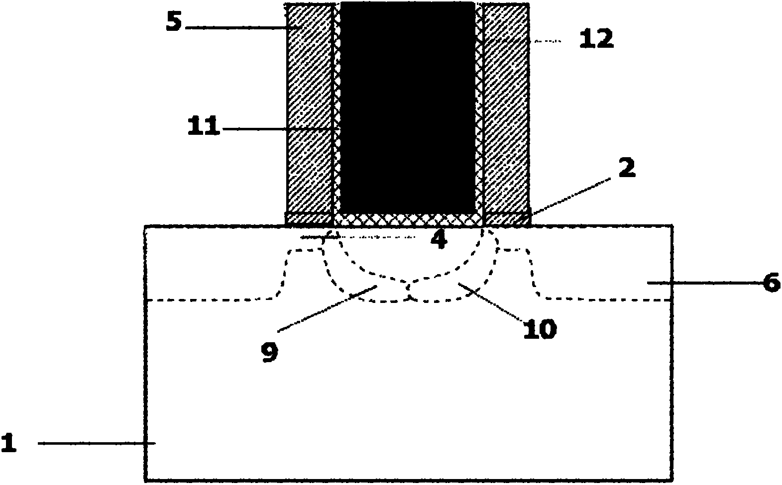
[0030] In the method of the MOS transistor provided by the present invention, a dummy gate electrode embedded in a thin film layer is formed on a substrate defining an active region to determine a channel region, and then the dummy gate electrode is removed to form a corresponding channel region. The shallow trench is used to carry out two symmetrical oblique ion implantation doping to the channel region through the shallow trench from directly above the channel region, so that heavy doped region.

[0031] In this embodiment, a high-K metal gate MOS transistor is taken as an example to further illustrate the present invention.

[0032] Please refer to figure 1 , the junction between the bottom of the channel region and the source and drain regions of the high-K metal gate MOS transistor is doped with the same type of impurity as...


PUM


Abstract

The invention discloses a manufacturing method of a high-K metal gate MOS (Metal Oxide Semiconductor) transistor, which comprises the following step: injecting corresponding impurities to the space right above a channel region of the MOS transistor, so that the bottom of the channel region of the MOS transistor and the junction between the channel region and a source drain region are heavily doped with impurities which are of the same type with the impurities doped on a substrate, the source drain region of the MOS transistor is doped with impurities of which the type is opposite to that of the impurities doped on the substrate, and the doping of the channel region can not cause impurity compensation to the source drain region. Thus, the manufactured transistor has an inversely doped channel which has a low surface concentration and a high bulk concentration, and can simultaneously satisfy the requirement for high drive current and the requirement of inhibiting the short-channel effect.

Description

technical field [0001] The invention relates to the technical field of semiconductor integrated circuits and its manufacture, in particular to a manufacturing method of a high-K metal gate MOS transistor. Background technique [0002] Metal-oxide-semiconductor field effect transistor (MOSFET for short) is the main device of modern integrated circuits. The rapid development of integrated circuits is mainly realized by continuously reducing the size of MOS devices and increasing the chip area. The benefits brought by the reduction of device size are that the channel resistance of the device is reduced, and the driving current of the device is increased, which leads to an increase in the speed of the circuit. At the same time, a smaller device scale can integrate more devices on a certain silicon chip area, which improves the integration of integrated circuits and reduces production costs. The scale of modern MOS devices has been reduced to the nanometer scale. Under this sc...

Claims


Application Information

Patent Timeline
Patent Type & Authority Applications(China)
IPC IPC(8): H01L21/336H01L21/265H01L29/10
Inventor 张盛东韩汝琦韩德栋
Owner PEKING UNIV SHENZHEN GRADUATE SCHOOL
Why Eureka
Try Eureka