Base material for printed circuit board

A technology for printed circuit boards and substrates, which is used in circuit substrate materials, printed circuit components, and secondary processing of printed circuits.

Inactive Publication Date: 2013-01-16
SUBTRON TECH
View PDF1 Cites 0 Cited by
  • Summary
  • Abstract
  • Description
  • Claims
  • Application Information

AI Technical Summary

Problems solved by technology

[0005] In order to solve this shortcoming, the method proposed by U.S. Patent No. 5,545,466 is to add a granular copper layer between the copper foil layer and the insulating substrate, but according to the disclosure of the patent, this method can only make etching Factor (Etch Factor) increased to 4 only
The solution proposed by China Taiwan Publication No. 200643224 patent application for invention is to provide a kind of etching solution with a faster etching rate. The shortcoming of this method is that this specific etching solution can only be applied to specific copper metal

Method used


Image

  • Base material for printed circuit board
  • Base material for printed circuit board
  • Base material for printed circuit board

Examples


Embodiment Construction

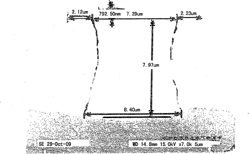
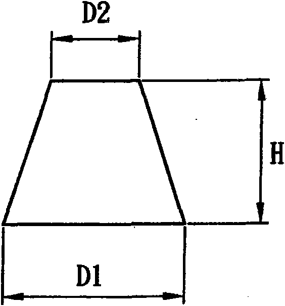
[0018] See first figure 2 , The base material used for printed circuit boards of the present invention is shown in FIG. 10 , which has a main layer 12 and a surface layer 14 . The main layer 12 can be a copper metal layer or a copper alloy layer. In this embodiment, its thickness is about 7.97um. The surface layer 14 is a nickel metal layer. In this embodiment, its thickness is about 0.792um. can be removed.

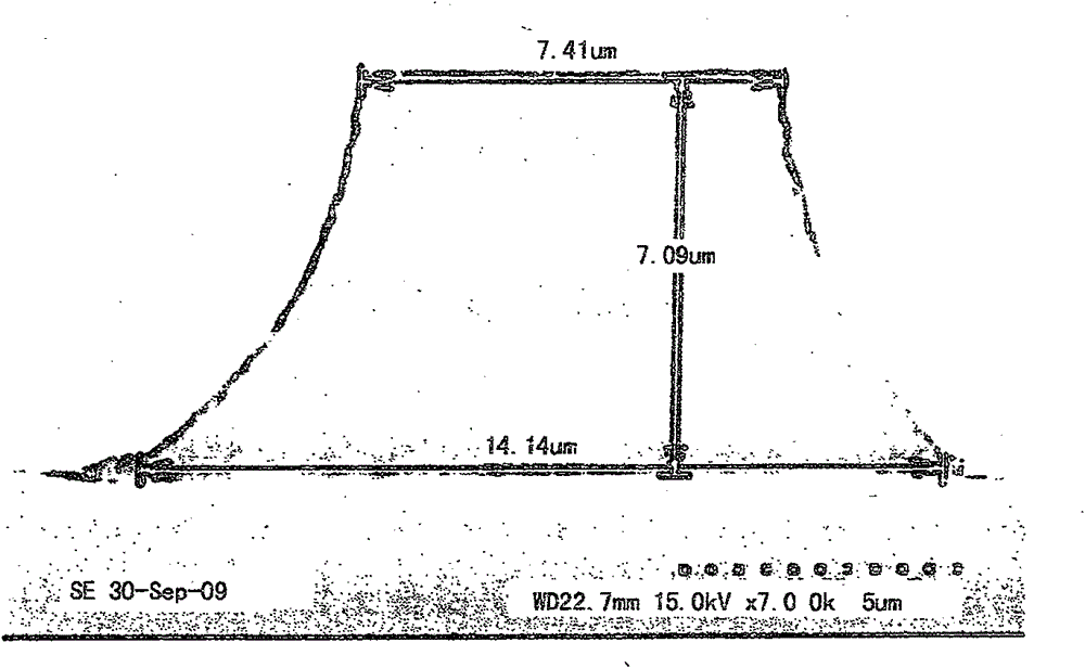
[0019] Such as image 3 As shown, in actual manufacturing, the main layer 12 is first arranged on an insulating substrate 20, and then the surface layer 14 is arranged on the surface of the main layer 12, wherein the arrangement method can be processes such as coating, attachment or electroplating, and then Then perform subsequent etching steps, such as coating the photoresist layer 30 , forming a circuit trace pattern mask layer, etching procedures, and removing the mask layer and the surface layer 14 . Of course, the complete substrate 10 can also be prepared in ad...


PUM

PropertyMeasurementUnit
thicknessaaaaaaaaaa

Abstract

The invention discloses a base material for a printed circuit board. The base material comprises a main layer and a surface layer which are made from different materials. The main layer is made of metal having good electrical conductivity and an upper surface. The surface layer is made of a material of which etching rate is smaller than that of the material of the main layer and arranged on the upper surface of the main layer. Therefore, the base material can provide a high-value etch factor when applied to a traditional etching solution.

Description

technical field [0001] The present invention relates to the construction of printed circuit boards (PCBs), and more particularly to a substrate for use with printed circuit boards. Background technique [0002] According to the manufacture of semiconductor integrated circuits, the circuit pattern on the printed circuit board or packaging substrate is usually formed by etching, and the wet etching method is the earliest etching technology adopted. Because this method is economical and convenient, it is currently Still used by most of the industry. The so-called wet etching method generally refers to arranging a conductive layer on the surface of a substrate, and covering the surface of the conductive layer to form a circuit pattern with an etching stopper layer, and then using a strong acid or alkali etching solution to The remaining conductive layer without the etch stop is removed leaving only the desired circuit traces. [0003] As we all know, the etchant used in the ab...

Claims


Application Information

Patent Timeline
Patent Type & Authority Patents(China)
IPC IPC(8): H05K1/03H05K3/38
Inventor 吴建男
Owner SUBTRON TECH
Why Eureka
Try Eureka