Lead frame for packaging, semiconductor packaging structure and packaging method

A lead frame and packaging method technology, which is applied in the fields of semiconductor devices, semiconductor/solid-state device manufacturing, semiconductor/solid-state device components, etc., can solve the problem of delamination of lead frame units and packaging resin, affecting the reliability of the packaging body, and increasing production costs and other problems, to achieve the effect of improving the effective utilization rate, not easy to decompose, and prolonging the service life

Pending Publication Date: 2021-03-19
NINGBO KANGQIANG ELECTRONICS CO LTD
View PDF7 Cites 0 Cited by
  • Summary
  • Abstract
  • Description
  • Claims
  • Application Information

AI Technical Summary

Problems solved by technology

However, these methods all require pre-plastic sealing of the lead frame, which adds a process of plastic sealing and deflashing. At the same time, each etching requires film attachment, mask alignment, exposure, and development. The increase in the process increases the production cost and the production cycle. extended while producing efficiencies
In addition, etching on the back side of the connection part is prone to lateral corrosion. Due to the small etching area, it is difficult to avoid this phenomenon by conventional etching methods, which may cause problems such as delamination of the lead frame unit and the packaging resin, affecting the integrity of the package. reliability

Method used


Image

  • Lead frame for packaging, semiconductor packaging structure and packaging method
  • Lead frame for packaging, semiconductor packaging structure and packaging method
  • Lead frame for packaging, semiconductor packaging structure and packaging method

Examples


Embodiment 1

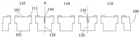
[0049] like figure 2 As shown, the lead frame 100 of this embodiment has an upper surface 101 (front side) and a lower surface 102 (back side), and includes a plurality of lead frame units 110 with a first electroplating layer 111 on the upper surface. The first electroplating layer 111 in this embodiment is a nickel-palladium-gold electroplating layer, and other metal materials with good solderability and conductivity can also be selected for replacement as required. There is a concave groove 130 between adjacent lead frame units, wherein the concave groove 130 is formed after half-etching the upper surface of the substrate, so the opening direction of the concave groove 130 is vertically upward, and the position below the substrate is The remainder of the surface remains to form the metal connection. In the figure, a virtual cutting line A represents a cutting line when cutting and separating the lead frame unit 110 .

[0050] The thickness of the frame body in this embod...

Embodiment 2

[0052] This embodiment provides a method for preparing the lead frame in Embodiment 1, including the following steps:

[0053] Prepare the degreased, cleaned and dried copper substrate as the frame body, paste the dry film on the upper surface 101 and the lower surface 102 of the substrate, and remove the dry film on the local area of ​​the upper surface of the substrate through mask alignment, exposure and development , electroplating nickel-palladium-gold on the substrate to form a first electroplating layer 111 on a local area of ​​the upper surface; the electroplating process is a prior art, and will not be repeated here;

[0054] After electroplating, the substrate is stripped, cleaned, dried, and then laminated again. An etching hole is formed in the middle of the substrate through a conventional etching process to form a patterned lead frame, exposing the side wall 113 inside the lead frame unit 110. Each lead frame unit 110 have the same line pattern on the upper surfa...

Embodiment 3

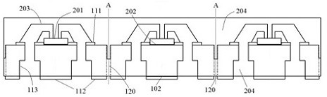
[0058] This embodiment provides a semiconductor package structure 200, including: a plurality of lead frame units 110, adjacent lead frame units are connected through the plastic sealing part 204, wherein the upper surface of the lead frame unit 110 has a first coating on the plastic sealing part 204 An electroplating layer 111, the lower surface of the lead frame machine unit 110 has an exposed second electroplating layer 112; the upper surface 101 of the lead frame unit is also equipped with a semiconductor chip 201, and the semiconductor chip 201 is connected to the corresponding lead frame unit 110 through a gold wire 203 The first electroplating layer 111 of the present embodiment is a nickel-palladium-gold electroplating layer; the plastic sealing part 204 covers the semiconductor chip 201, the lead wire 203 and the lead frame unit 110, wherein the plastic sealing part is made of epoxy resin (EMC) material .


PUM

PropertyMeasurementUnit
Thicknessaaaaaaaaaa
Thicknessaaaaaaaaaa

Abstract

The invention belongs to the technical field of semiconductor devices, and particularly relates to a lead frame for packaging, a semiconductor packaging structure and a packaging method. The lead frame comprises a plurality of lead frame units, a concave groove is formed between every two adjacent lead frame units, and the opening direction of each concave groove is vertically upward. According tothe invention, the upper surface of a substrate is treated by an acidic etching solution to remove part of the thickness between the lead frame units to form the concave grooves, and then the residual metal connecting part of the substrate is removed by an alkaline etching solution after plastic package, so that an ideal etching effect is achieved by controlling the technological conditions of alkaline etching, the adjacent packaging units are connected only through the plastic packaging material without metal connection, an overall test can be carried out before cutting, the test flow of a single packaging body is simplified, the product detection efficiency is improved, the abrasion of a metal material of the lead frame to a cutting tool is avoided, the service life of the cutting toolis prolonged, and the production cost is reduced.

Description

technical field [0001] The invention belongs to the technical field of semiconductor devices, and in particular relates to a lead frame for packaging, a semiconductor packaging structure and a packaging method. Background technique [0002] The development of semiconductor packaging technology is becoming more and more mature, and its application is becoming more and more extensive. Among them, the lead frame is used as the chip carrier of integrated circuits. It realizes the connection between the chip and the electrical signal of the external circuit board by means of bonding materials. important components. [0003] The current semiconductor packaging process mainly includes steps such as chip bonding, chip cutting, chip welding, bonding, plastic sealing, laser printing, electroplating, lead frame film bonding, and unit cutting. Since there are still metal connections between the lead frame units, the entire package structure cannot be tested. It is usually necessary to ...

Claims


Application Information

Patent Timeline
IPC IPC(8): H01L23/495H01L21/48H01L21/56
CPCH01L23/49548H01L21/4821H01L21/4828H01L21/561H01L2224/48257H01L2224/73265H01L2224/48095H01L2224/32245H01L2224/48247H01L2924/181H01L2224/97H01L2924/00012
Inventor 黎超丰冯小龙章新立林渊杰林杰
Owner NINGBO KANGQIANG ELECTRONICS CO LTD
Why Eureka
Try Eureka