Schottky barrier diode and method for manufacturing schottky barrier diode
A Schottky barrier diode technology, applied in semiconductor devices, electrical components, circuits, etc., can solve the problems of ineffective enhancement of Schottky barrier diode withstand voltage, poor crystallinity, etc., to reduce reverse Leakage current, effect of reducing dislocation density
- Summary
- Abstract
- Description
- Claims
- Application Information
AI Technical Summary
Problems solved by technology
Method used
Image

Examples
no. 1 example
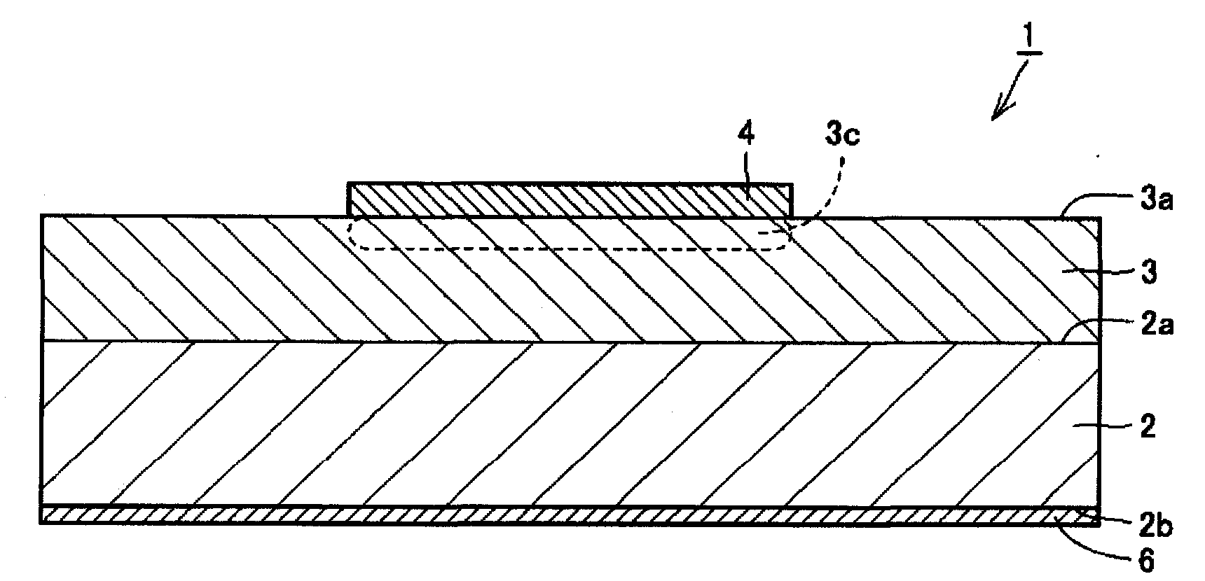
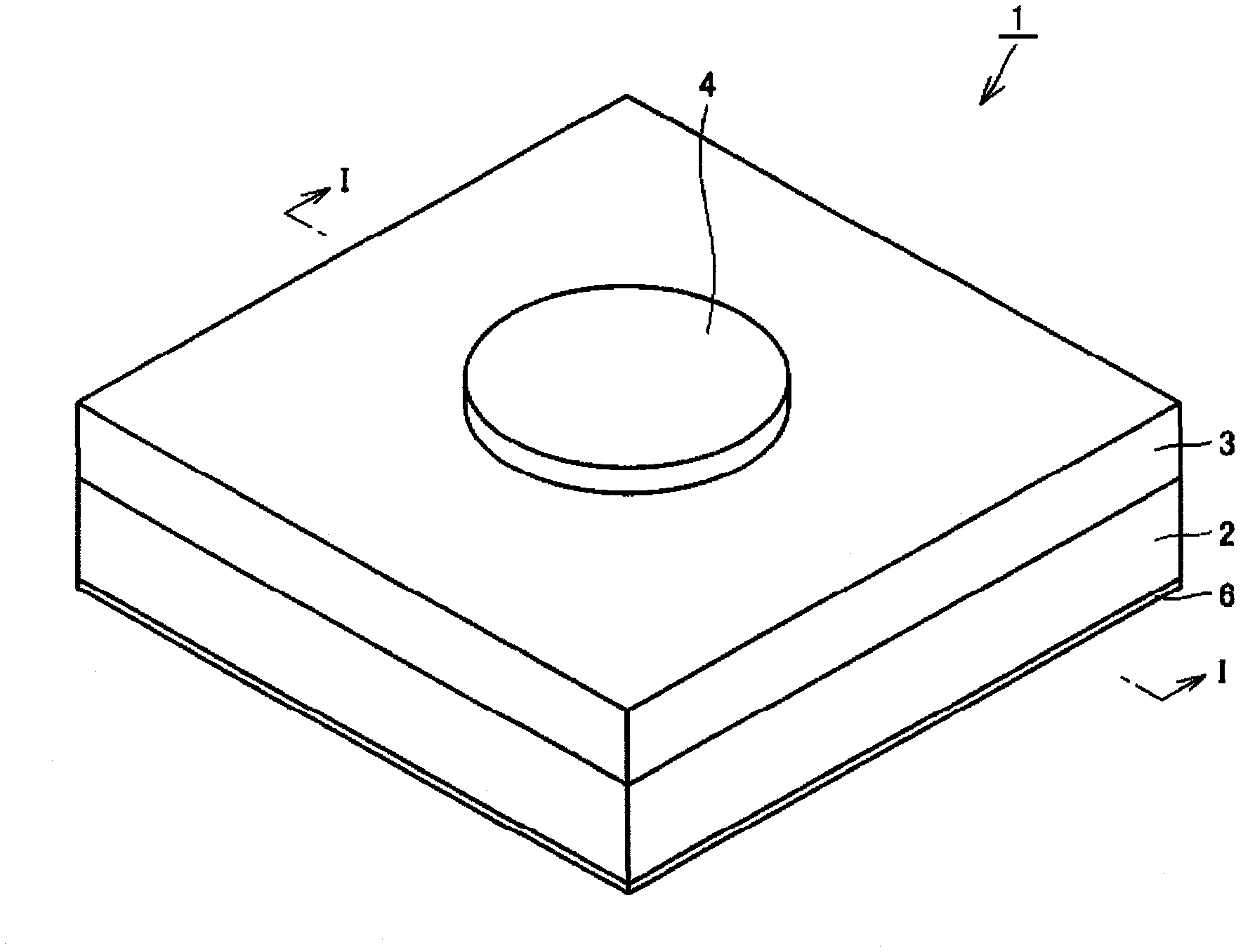
[0060] figure 1 is a cross-sectional view schematically showing the Schottky barrier diode in this embodiment. figure 2 is a perspective view schematically showing the Schottky barrier diode in this embodiment. Notice, figure 1 is along figure 2 A cross-sectional view taken along line I-I in . Such as figure 1 and 2 As shown, a Schottky barrier diode (SBD) 1 includes a GaN substrate 2, a GaN layer 3 formed on the front surface 2a of the GaN substrate 2, a Schottky electrode 4 formed on the GaN layer 3, and a GaN layer formed on the GaN layer 3. Ohmic electrode 6 on back surface 2 b of GaN substrate 2 .
[0061] GaN substrate 2 has front surface 2a and back surface 2b. It is preferable that GaN substrate 2 has a low dislocation density. For example, GaN substrate 2 has a preferred 1×10 8 cm -2 or smaller, more preferably 1×10 7 cm -2 or less, and even more preferably 1×10 6 cm -2 or smaller dislocation density. It is also possible to reduce the dislocation dens...
no. 2 example
[0091] Figure 5 is a cross-sectional view schematically showing a Schottky barrier diode in this embodiment. Figure 6 is a partial sectional view schematically showing the Schottky barrier diode in this embodiment. Notice, Figure 5 is along Figure 6 A cross-sectional view taken along line V-V in . Such as Figure 5 and 6 As shown, the difference of the Schottky barrier diode 11 in this embodiment is that: the Schottky barrier diode 11 further includes a field plate (FP) electrode 16 and an insulating layer 17 .
[0092] Specifically, insulating layer 17 is formed on front surface 3 a of GaN layer 3 , and has an opening in which Schottky electrode 4 is formed. The insulating layer 17 is made of, for example, a silicon nitride film (SiN x ) etc. to construct.
[0093] Field plate electrode 16 is formed to be connected to Schottky electrode 4 in the opening of insulating layer 17 and to overlap insulating film 17 . For example, the field plate electrode 16 has a ring...
no. 3 example
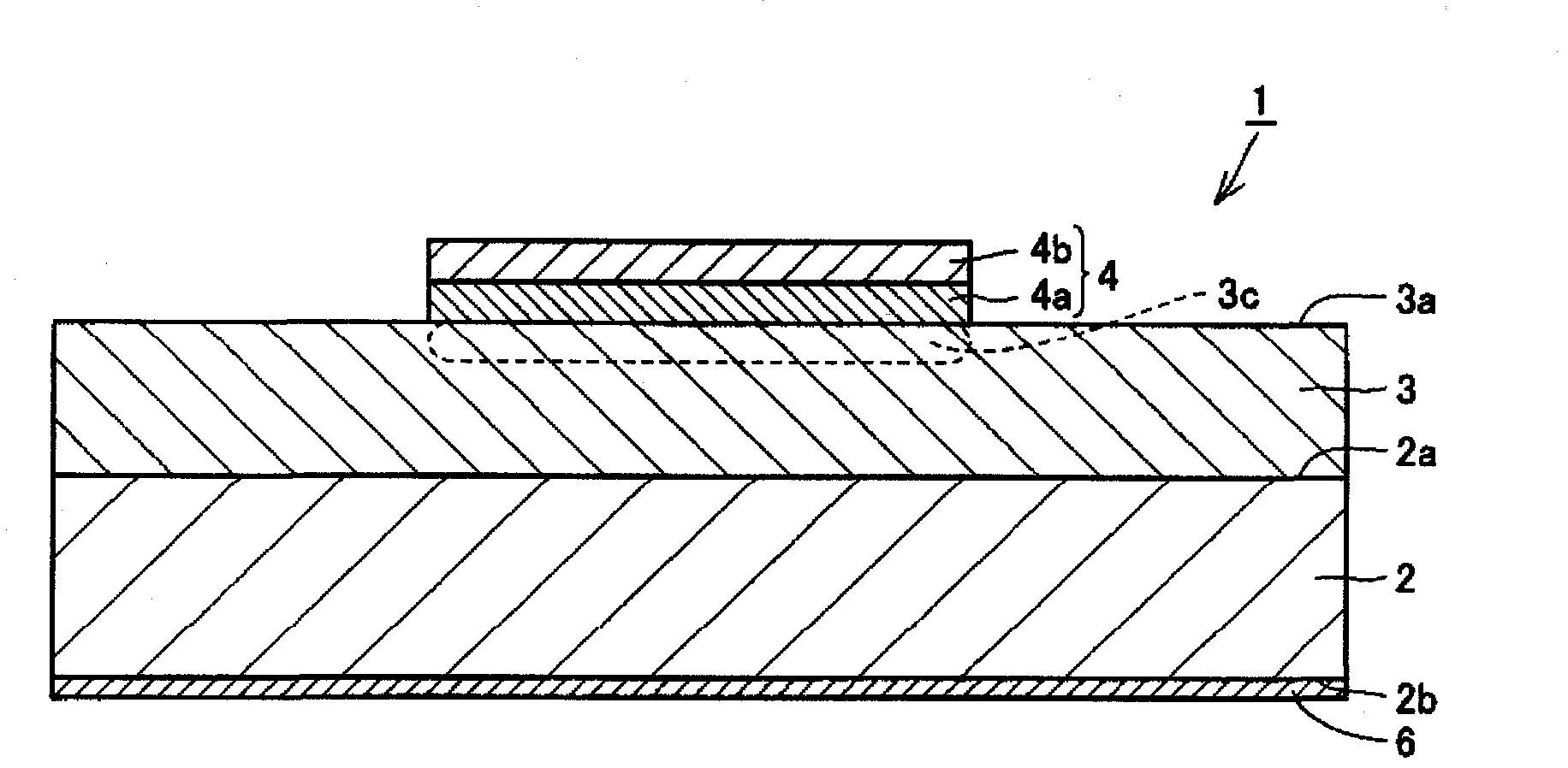
[0124] Figure 8 is a cross-sectional view schematically showing a Schottky barrier diode in this embodiment. refer to Figure 8 , the Schottky barrier diode 21 in this embodiment has a configuration basically similar to that of the Schottky barrier diode 11 in the second embodiment. The Schottky barrier diode 21 in this embodiment is different in that the Schottky barrier diode 21 does not include a GaN substrate.
[0125] Specifically, the Schottky barrier diode 21 includes a support substrate 23 , a GaN substrate 22 , a GaN layer 3 , an electrode 15 , an insulating layer 17 and an ohmic electrode 6 . The region 3c of the GaN layer 3 in contact with the Schottky electrode 4 has a 1×10 8 cm -2 or smaller, preferably 1×10 7 cm -2 or less, and more preferably 1×10 6 cm -2 or smaller dislocation density.
[0126] The support substrate 23 is a conductive substrate. GaN base 22 is formed on this support substrate 23 . GaN layer 3 is formed on this GaN substrate 22 . No...
PUM
| Property | Measurement | Unit |
|---|---|---|
| diameter | aaaaa | aaaaa |
| thickness | aaaaa | aaaaa |
| thickness | aaaaa | aaaaa |
Abstract
Description
Claims
Application Information