Method for preparing large-scale two-dimensional nanomaterial graphite

A two-dimensional nanomaterial, large-scale technology, applied in the preparation of two-dimensional nanomaterial graphene, using carbon element injection to prepare large-scale graphene, achieving large size, saving development and equipment costs, and large size effects

Inactive Publication Date: 2011-07-13
SOUTHEAST UNIV
View PDF2 Cites 47 Cited by
  • Summary
  • Abstract
  • Description
  • Claims
  • Application Information

AI Technical Summary

Problems solved by technology

[0005]Technical problem: the technical problem to be solved by the present invention is to propose a method for preparing a large-scale two-dimensional nanomaterial graphene, and prepare graphene by injecting carbon elements film to overcome the disadvantages of many existing methods, such as graphene ruler

Method used


Image

  • Method for preparing large-scale two-dimensional nanomaterial graphite
  • Method for preparing large-scale two-dimensional nanomaterial graphite
  • Method for preparing large-scale two-dimensional nanomaterial graphite

Examples


Embodiment 1

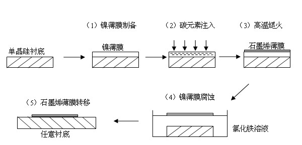
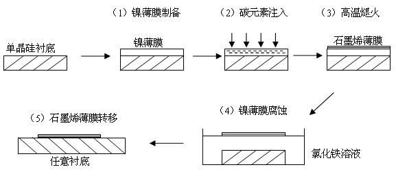
[0024] Embodiment 1: implement according to the following five steps

[0025] 1. Nickel thin film preparation: use sputtering method (Sputtering) to coat a uniform nickel thin film on the surface of a single crystal silicon wafer (0.7mm thick), with a thickness of 300nm.

[0026] 2. Carbon element implantation: The carbon element is implanted into the nickel film by means of ion implantation. The ion implantation energy is 600eV, and the dose is 5x10 15 cm -2 ,

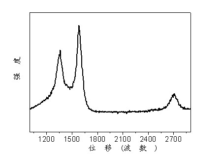
[0027] 3. High-temperature annealing: put the sample injected with carbon into a high-temperature furnace for annealing, and the annealing temperature is 900 o C, the annealing time is 30 minutes, the vacuum degree is 10 -5 Pa. And after cooling down to room temperature. At this point, a layer of graphene film will grow on the surface of the nickel film,

[0028] 4. Corrosion of nickel film: put the substrate with graphene film on the surface into ferric chloride solution for corrosion, the solution concentrat...

Embodiment 2

[0031] Embodiment 2: one, nickel thin film preparation: utilize sputtering method (Sputtering) to coat uniform nickel thin film on the surface of monocrystalline silicon chip (0.7 mm thick), thickness is 300nm,

[0032] 2. Carbon element implantation: The carbon element is implanted into the nickel film by means of ion implantation. The ion implantation energy is 1000 eV, and the metering is 10 16 cm -2 ,

[0033] 3. High-temperature annealing: put the sample injected with carbon into a high-temperature furnace for annealing, and the annealing temperature is 800 o C, the annealing time is 45 minutes, and the vacuum degree is 1Pa. And after cooling down to room temperature. At this point, a layer of graphene film will grow on the surface of the nickel film,

[0034] 4. Corrosion of nickel film: put the substrate with graphene film on the surface into ferric chloride solution for corrosion, the solution concentration is 1 mol / liter, and the corrosion time is 10 hours. At ...

Embodiment 3

[0037] 1. Nickel thin film preparation: use sputtering method (Sputtering) to coat a uniform nickel thin film on the surface of a single crystal silicon wafer (0.7 mm thick), with a thickness of 200nm.

[0038] 2. Carbon element implantation: The carbon element is implanted into the nickel film by means of ion implantation. The energy of ion implantation is 600eV, and the metering is 5x10 15 cm -2 ,

[0039] 3. High-temperature annealing: put the sample injected with carbon into a high-temperature furnace for annealing, and the annealing temperature is 1000o C, the annealing time is 15 minutes, the vacuum degree is 10 -5 Pa. And after cooling down to room temperature. At this point, a layer of graphene film will grow on the surface of the nickel film,

[0040] 4. Corrosion of nickel film: put the substrate with graphene film on the surface into ferric chloride solution for corrosion, the solution concentration is 0.5 mol / liter, and the corrosion time is 24 hours. At thi...


PUM

PropertyMeasurementUnit
thicknessaaaaaaaaaa
thicknessaaaaaaaaaa
thicknessaaaaaaaaaa

Abstract

The invention relates to a method for preparing a large-scale two-dimensional nanomaterial graphite, comprising the following steps of: plating a nickel film with the thickness of 100-300nm on the surface of monocrystal silicon, and then injecting carbon element into the nickel film by adopting an ion implantation mode; annealing for 15min-1h at a high temperature between 600 DEG C and 1,000 DEG C and a vacuum degree of from (10-5)Pa to 1Pa, and cooling to room temperature so that carbon atoms are separated out from the nickel film and recombined. Therefore, a layer of graphite film (the film thickness depends on various experiment parameters, such as carbon injection content, and the like) can be formed on the surface of the nickel film. When a sample is put into a FeCl3 solution, the nickel film can be corroded, and the graphite film can be separated out and floats on the surface of the liquid; and at the moment, the graphite film can be transferred away from the liquid with any substrate. Therefore, the large-scale graphite film with the size of several centimeters can be prepared.

Description

technical field [0001] The invention relates to a preparation method of two-dimensional nano material graphene, and a preparation process thereof, in particular to a method for preparing large-scale graphene by injecting carbon elements, and a preparation process thereof. The invention belongs to the technical field of materials. Background technique [0002] Graphene is a two-dimensional crystal composed of carbon atoms, and some people use "single-layer graphite" as its name. In graphene, carbon atoms are represented by sp 2 Hybridized and arranged into a honeycomb hexagonal planar structure. Graphene is also the basic building block of other carbon material allotropes. [0003] Graphene was first discovered by scientists from the University of Manchester in 2004, and the discoverer of graphene won the Nobel Prize in Physics in 2010. Room temperature mobility of carriers in graphene >20000 cm 2 / Vs, which is higher than any semiconductor material known so far, incl...

Claims


Application Information

Patent Timeline
Patent Type & Authority Applications(China)
IPC IPC(8): C01B31/04
Inventor 倪振华詹达申泽骧丁荣
Owner SOUTHEAST UNIV
Why Eureka
Try Eureka