Eureka AIR delivers breakthrough ideas for toughest innovation challenges, trusted by R&D personnel around the world.

Method and device for coupling and purifying polysilicon and removing phosphorus and metal with electron beams

A polysilicon and electron beam technology, applied in non-metallic elements, chemical instruments and methods, silicon compounds, etc., can solve the problems of high energy consumption and uneven distribution of impurities, and achieve the effects of energy saving, low cost and fast removal speed.

Inactive Publication Date: 2011-07-13
谭毅
View PDF5 Cites 17 Cited by
  • Summary
  • Abstract
  • Description
  • Claims
  • Application Information

AI Technical Summary

Problems solved by technology

The known invention patent with application number 200810011631.8 uses induction heating and electron beams to achieve the purpose of removing phosphorus and metal impurities in polysilicon, but the disadvantage of this method is that additional induction heating is used, which consumes a lot of energy and uses a block Silicon material is smelted and purified, and the impurity distribution is relatively uneven

Method used


Image

  • Method and device for coupling and purifying polysilicon and removing phosphorus and metal with electron beams
  • Method and device for coupling and purifying polysilicon and removing phosphorus and metal with electron beams

Examples


Embodiment 1

[0021] A method for the coupled purification of polysilicon by electron beam dephosphorization and metal removal. First, a stable molten pool is formed on the top of a low-phosphorus, low-metal high-purity silicon ingot through an electron beam, and then the silicon powder to be purified is dropped into the molten pool for melting , realize rapid melting of powder to remove volatile impurity phosphorus in silicon powder, and at the same time carry out directional ingot pulling to enable directional solidification and growth of low-phosphorus polysilicon, and remove metal impurities in polysilicon through segregation effect. The specific steps are as follows:

[0022] The first step of material preparation: use low-phosphorus, low-metal high-purity silicon ingots in vacuum equipment as carriers, and put high-phosphorus and high-metal powder silicon materials that need to be purified into powder buckets on top of them;

[0023] The second step of pretreatment: vacuumize the vacuu...

Embodiment 2

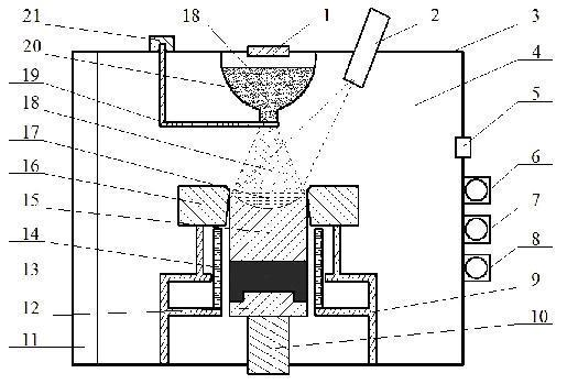
[0026] Such as figure 1The equipment used in the coupling purification method of polysilicon by electron beam dephosphorization and metal removal is shown. The equipment adopts a vacuum cover 11, a vacuum furnace wall 3 and a powder filling cover 1 to form a vacuum equipment, and the inner chamber of the vacuum equipment is a vacuum chamber 4; The upper part of the vacuum chamber is equipped with a powder loading bucket, the top of the powder loading bucket is equipped with a powder loading cover, the powder loading cover is located on the vacuum furnace wall, the bottom of the powder loading bucket has a discharge port, and the discharge port is equipped with an externally driven powder baffle. The externally driven powder baffle is an L-shaped powder baffle. One end of the powder baffle is rotated and installed in the rotating mechanism. The rotating mechanism is installed outside the vacuum furnace wall. A crucible is installed at the bottom of the outlet of the powder loadi...

Embodiment 3

[0028] Adopt the equipment described in embodiment 2 to carry out the method for the coupling purification polysilicon of electron beam dephosphorization, metal removal, specifically:

[0029] The first step of material preparation: put the low-phosphorus, low-metal high-purity silicon ingot 15 with a phosphorus content of 0.00004% and a total metal content of 0.0002% on the graphite block 8, and the top of the low-phosphorus, low-metal high-purity silicon ingot 15 is connected with the water-cooled copper The upper surface of the annular crucible 16 should be horizontal, and the powder baffle plate 19 should be rotated to the bottom of the powder loading bucket 20 by the rotating mechanism 21 to block the powder falling hole at the bottom of the powder loading bucket 20, and open the powder loading cover 1 to the powder loading bucket 20 Add phosphorus content 0.003%, metal impurity total content 0.01% high phosphorus, high metal silicon powder 18, high phosphorus, high metal ...


PUM


Abstract

The invention belongs to the technical field of polysilicon purification with a physical metallurgy technology and particularly relates to a method for coupling and purifying polysilicon and removing phosphorus and metal with electron beams. The method comprises the following steps of: forming a stable melting pool on the top of a low-phosphorous low-metal high-purity silicon ingot with the electron beams; putting silicon powder to be purified into the melting pool and melting to realize the rapid melting of the powder body to remove volatile phosphorous impurity in the silicon powder; simultaneously carrying out directional ingot pulling so that the low-phosphorus polysilicon grows in a directional solidification way; and removing metal impurities in the polysilicon by utilizing a segregation effect. The invention has the remarkable effects that: because ways of melting silicon powder with the electron beams and carrying out directional solidification are simultaneously adopted, the phosphorus impurity is rapidly removed with the electron beams, and the metal impurities with lower segregation coefficient are removed by the directional solidification way, the purity of the polysilicon is effectively improved, and the using requirement of solar grade silicon is achieved. The invention has the advantages of good purification effect, stable technology, simple process, high production efficiency, energy saving, low cost and suitability for batch production.

Description

technical field [0001] The invention belongs to the technical field of polysilicon purification by physical metallurgy technology, and particularly relates to a purification method for removing phosphorus and metal impurities in polysilicon by using electron beams. Background technique [0002] As an important part of renewable energy, solar power generation has become one of the main ways to achieve low-carbon goals. However, due to the limitation of the production cost of solar-grade polysilicon, an important raw material for solar cells, the installed capacity of solar power generation in my country is not high. As of 2008 At the end of the year, the total installed capacity of solar cells in the country was only 300MW, which was less than the amount added in a year in Germany. The high manufacturing cost and complex manufacturing process of solar-grade polysilicon are the bottlenecks restricting the development of the photovoltaic industry, which seriously hinders the pro...

Claims


Application Information

Patent Timeline
Patent Type & Authority Applications(China)
IPC IPC(8): C01B33/037
CPCY02P20/10
Inventor 谭毅姜大川邹瑞洵
Owner 谭毅
Why Eureka
Eureka Blog
Learn More