Mobile semiconductor laser mould repairing system

A laser repair and semiconductor technology, which is applied in laser welding equipment, manufacturing tools, welding equipment, etc., can solve the problems of inconvenient movement and bulky laser repair device, and achieve the effect of eliminating time-consuming and laborious work, shortening repair time, and realizing repair

Inactive Publication Date: 2011-07-20
HUNAN UNIV
View PDF0 Cites 11 Cited by
  • Summary
  • Abstract
  • Description
  • Claims
  • Application Information

AI Technical Summary

Problems solved by technology

[0005] The technical solution adopted by the patent of this invention to solve its technical problems is: Aiming at the shortcomings of the current laser repair device, which are bulky and inconvenient to move, this patent has invented a mobile semiconductor laser mold surface repair system, which is characterized by high Integration of power semiconductor lasers, 6-axis fully articulated robots and coaxial powder nozzles

Method used


Image

  • Mobile semiconductor laser mould repairing system

Examples


Embodiment Construction

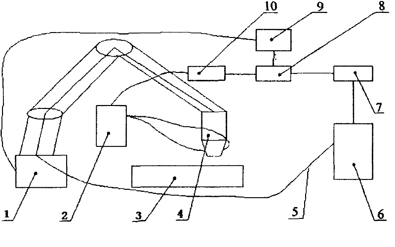
[0011] In conjunction with the accompanying drawings, the specific implementation process is as follows:

[0012] 1) Before the laser repair starts, the damaged part of the workpiece 3 is firstly preprocessed, and the three-dimensional solid model of the damaged part is scanned and extracted;

[0013] 2) The CAD model is layered by layering software to obtain the STL file;

[0014] 3) Input material thermophysical parameters, environmental parameters and other data related to process parameter design into the system, and then generate the processing path and CNC code of each layer according to the STL file;

[0015] 4) The computer 8 sends powder feeding instructions to the powder feeding controller 10 to control the opening of the powder feeder 2 and its powder feeding rate; sends power instructions to the laser controller 7 to control the opening of the semiconductor laser 6 and its power output; The device 9 transmits speed commands to control the scanning path and scannin...


PUM


Abstract

The invention discloses a high-efficiency flexible laser repairing system for a mould in a complicated shape. The system integrates a high-power semiconductor laser device, 6-axis full-joint type industrial robot, an optical fiber light guiding system and the like. According to the invention, as a semiconductor laser device with small volume and light weight and a movably-mounted industrial robot are adopted, the movement of the entire system can be realized conveniently so as to realize field repair of the mould. The invention provides a method for integrating the semiconductor laser device, the industrial robot, a laser working head and the like, and the method comprises the following steps: transmitting semiconductor laser through the optical fiber light guiding system which has good flexibility and is flexible and convenient; after the semiconductor laser reaches the laser working head held in the wrist of the industrial robot, collimating and focusing the semiconductor laser and irradiating the damaged part; and meanwhile, heating the powder and workpiece surface material, and cladding the repaired part layer by layer under the program control to realize repair of the damaged part. According to the invention, the field processing of large and ultra-large moulds or parts which are inconvenient to move can be realized, and the system disclosed by the invention is particularly suitable for flexible production of multiple varieties and batches.

Description

technical field [0001] The invention relates to equipment for repairing and maintaining damaged parts, in particular to equipment for repairing large molds on site. Background technique [0002] Currently available repair techniques include electroplating, arc or flame surfacing, thermal spraying (flame, plasma), etc. The electroplating layer is generally very thin, no more than 0.03mm, and it is poorly bonded to the substrate, and it is difficult to repair the damaged part of the shape; during surfacing welding, thermal spraying or spray welding, the heat injection is large, the energy is not concentrated, the heat affected area of ​​the mold is large, and it is easy to be deformed Even cracking, the dilution rate of the sprayed layer is large, which reduces the performance of the matrix and the material, and the combination of the repaired part and the matrix of the part is difficult to meet the requirements of the original part. Compared with the existing repair technolo...

Claims


Application Information

Patent Timeline
Patent Type & Authority Applications(China)
IPC IPC(8): B23P6/00B23K26/00B23K26/342
Inventor 刘继常钟志华范滇元
Owner HUNAN UNIV
Why Eureka
Try Eureka