Step array high-voltage light-emitting diode and preparation method thereof

A high-voltage light-emitting, stepped technology, applied in semiconductor devices, electrical components, circuits, etc., can solve the problems of poor heat dissipation and complicated process of array-type high-voltage light-emitting tubes

Inactive Publication Date: 2011-07-20
JILIN UNIV +2
View PDF4 Cites 10 Cited by
  • Summary
  • Abstract
  • Description
  • Claims
  • Application Information

AI Technical Summary

Problems solved by technology

[0004] The purpose of the present invention is to provide a new stepped array high-voltage luminous tube and its preparation method to solve the problems of poor heat dissipation and complicated process of the above-mentioned arrayed high-voltage luminous tubes

Method used


Image

  • Step array high-voltage light-emitting diode and preparation method thereof
  • Step array high-voltage light-emitting diode and preparation method thereof
  • Step array high-voltage light-emitting diode and preparation method thereof

Examples


Embodiment 1

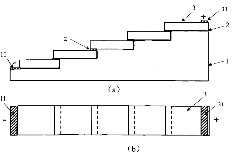
[0047] Ladder array high voltage luminous tubes. The structure of this new stepped array high-voltage light-emitting tube is shown in the attached figure 2 , its preparation process is:

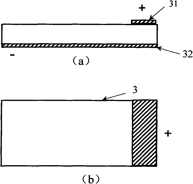
[0048] A. The unit die 3 selects the GaN light-emitting tube epitaxial wafer prepared by n-type conductive SiC substrate; first prepares the upper electrode on the light-emitting surface, and the preparation method can be thermal evaporation, electron beam evaporation, and magnetron lasing method The strip-shaped upper electrode 31 is prepared by a mask method or photolithography and photoresist stripping process; the area of ​​the strip-shaped upper electrode 31 accounts for 5-30% of the upper surface area of ​​the entire unit tube core; the metal material of the electrode Binary alloy materials such as Au, NiAu, TiAu, ZnAu or PtAu can be used, and ternary alloy materials such as TiPtAu, TiNiAu or NiPtAu can also be used; and then alloyed and thinned by conventional processes, the substrat...

Embodiment 2

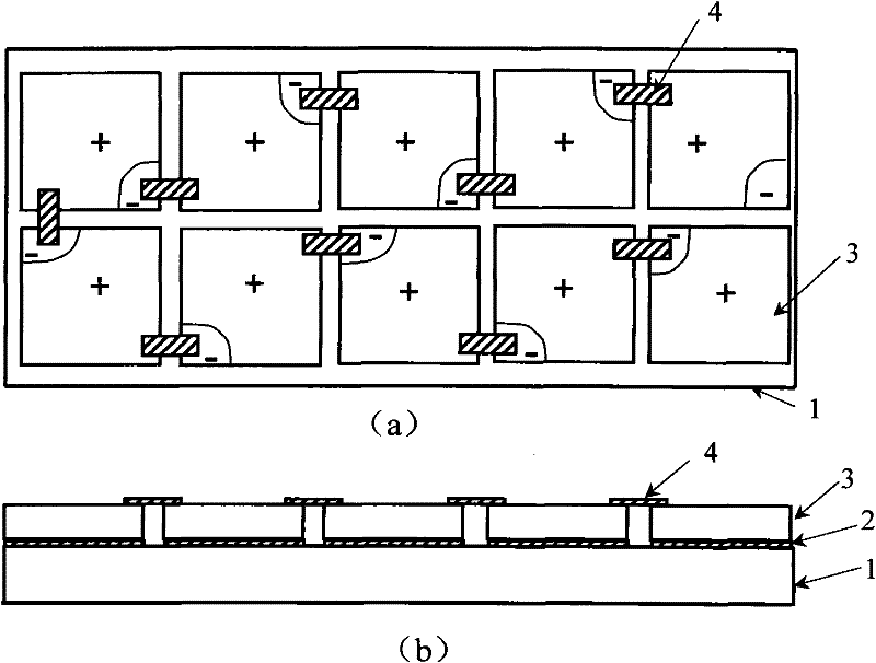
[0052] Cross-shaped step-array high-voltage light-emitting tubes. The structure of this cross-shaped step-array high-voltage light-emitting tube is shown in the appendix Figure 7, the selection of the unit tube core 3 and the preparation of the electrodes in the preparation process, as well as the sintering process for preparing the stepped array high-voltage light-emitting tube are the same as in the embodiment 1; Metallized bridging lines 12 should be prepared on the slope between them; after sintering and preparing each unit ladder array type high-voltage light-emitting tube, the electrode of the tube core on one unit ladder and the electrode of the tube core on the other unit ladder are electrically bridged and connected. ; Now think that improving the operating voltage, the series bridge connection method is an example, and the bridging connection method is described as follows: the upper electrode of the left unit ladder die is bonded to the metallized bridge wire 12 co...


PUM


Abstract

The invention belongs to the technical field of semiconductor luminescent devices and preparation thereof, and particularly relates to a gallium nitride (GaN)-based array high-voltage light-emitting diode and a preparation method thereof. The light-emitting diode consists of a support substrate 1, soldering terminals 2 on the support substrate 1 and unit tube cores 3 on the soldering terminals 2,and is characterized in that the unit tube cores 3 have a vertical structure, an upper electrode 31 of each unit tube core is in a strip shape, and a lower electrode 32 is covered on the lower side of all the unit tube cores 3; the support substrate 1 has a step structure in the one-dimensional direction, and a metalized film 11 is arranged on each step; and the unit tube core 3 is formed on eachstep of the support substrate 1, the unit tube cores 3 are welded and fixed on the support substrate 1 by the soldering terminals 2, the lower electrode 32 of one unit tube core on the upper side is welded on the upper electrode 31 of the unit tube core on the lower side simultaneously, and a plurality of unit tube cores are welded in series to form the step array high-voltage light-emitting diode. By the step array high-voltage light-emitting diode, the defects that a face-up structure is poor in heat dissipation and a preparation process for bridge electrodes is complex are overcome, and the application range of the high-voltage light-emitting diode is expanded further.

Description

technical field [0001] The invention belongs to the technical field of semiconductor light-emitting devices and their preparation, and in particular relates to a GaN-based array type high-voltage light-emitting tube and a preparation method thereof. Background technique [0002] With the breakthrough of the third-generation semiconductor material gallium nitride and the advent of blue, green, and white light-emitting diodes, following the microelectronics revolution triggered by semiconductor technology, a new industrial revolution-the lighting revolution is being bred, and its symbol is the semiconductor Lamps will gradually replace incandescent and fluorescent lamps. Because semiconductor lighting (also known as solid-state lighting) has the advantages of energy saving, long life, maintenance-free, and environmental protection, it is generally believed in the industry that, just like transistors replace electron tubes, semiconductor lamps replace traditional incandescent l...

Claims


Application Information

Patent Timeline
Patent Type & Authority Applications(China)
IPC IPC(8): H01L25/075H01L33/40H01L33/48H01L33/62H01L33/00
Inventor 杜国同梁红伟彭晖郭文平闫春辉
Owner JILIN UNIV
Why Eureka
Try Eureka