Copper-doped perovskite thin film, in-situ preparation method and solar cell device without hole transport layer

An in-situ preparation and perovskite technology, which is applied in the direction of electrical solid devices, electrical components, semiconductor devices, etc., can solve the problems of high cost, high cost of hole transport layer, low photoelectric conversion efficiency of perovskite solar cells, etc. , to achieve the effect of reducing energy consumption, reducing cost, and the preparation method is simple and controllable

Active Publication Date: 2019-08-23
XUCHANG UNIV
View PDF6 Cites 0 Cited by
  • Summary
  • Abstract
  • Description
  • Claims
  • Application Information

AI Technical Summary

Problems solved by technology

[0009] In view of the deficiencies in the prior art: the photoelectric conversion efficiency of perovskite solar cells is not high, the cost is high, especially the problem that the cost of the hole transport layer is high, the technical problem to be solved by the present invention is to provide a copper-lead content ratio composed of copper Copper-doped perovskite film gradually decreasing from the surface to the bottom of the doped perovskite film, and a solar cell comprising the copper-doped perovskite film

Method used


Image

  • Copper-doped perovskite thin film, in-situ preparation method and solar cell device without hole transport layer
  • Copper-doped perovskite thin film, in-situ preparation method and solar cell device without hole transport layer
  • Copper-doped perovskite thin film, in-situ preparation method and solar cell device without hole transport layer

Examples


Embodiment 1

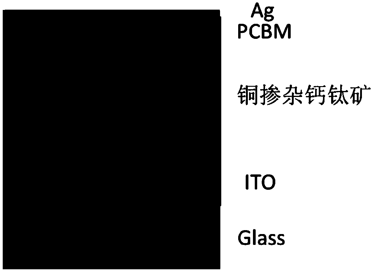
[0054] (1) Substrate cleaning: Clean the ITO glass ultrasonically with detergent for 30 minutes, then rinse it with deionized water, then ultrasonically clean it with acetone for 30 minutes, then ultrasonically clean it with absolute ethanol for 30 minutes, and finally dry it with a nitrogen gun and use ultraviolet light to clean it. Irradiate for 2 minutes;

[0055] (2) Cuprous iodide: Use vacuum evaporation technology to vapor-deposit a 10nm-thick elemental copper film on the cleaned ITO conductive glass, then add elemental iodine particles in a closed container, and then deposit the ITO conductive glass with a copper film Put it in and keep it at 25°C for 1-5min until the copper reacts completely;

[0056] (3) Copper-doped perovskite layer: Under oxygen-barrier and anhydrous conditions such as a glove box, take lead acetate and CH with a molar ratio of 1:3 3 NH 3 I was dissolved in N,N-dimethylformamide to prepare 1mol / L CH 3 NH 3 PB 3 solution, the CH 3 NH 3 PB 3 T...

Embodiment 2

[0059] (1) Substrate cleaning: Clean the ITO glass ultrasonically with detergent for 30 minutes, then rinse it with deionized water, then ultrasonically clean it with acetone for 30 minutes, then ultrasonically clean it with absolute ethanol for 30 minutes, and finally dry it with a nitrogen gun and use ultraviolet light to clean it. Irradiate for 2 minutes;

[0060] (2) Cuprous iodide: Use vacuum evaporation technology to vapor-deposit a 20nm-thick elemental copper film on the cleaned ITO conductive glass, add elemental iodine particles into the airtight container, and then conduct the ITO of the deposited copper film Put the glass in and keep it at 25°C for 1-5min until the copper reacts completely;

[0061] (3) Copper-doped perovskite layer: under the condition of oxygen barrier and anhydrous, take lead acetate and CH with a molar ratio of 1:3 3 NH 3 I was dissolved in N,N-dimethylformamide to prepare 1mol / L CH 3 NH 3 PB 3 solution, the CH 3 NH 3 PB 3 The solution w...

Embodiment 3

[0064] (1) Substrate cleaning: Clean the ITO glass ultrasonically with detergent for 30 minutes, then rinse it with deionized water, then ultrasonically clean it with acetone for 30 minutes, then ultrasonically clean it with absolute ethanol for 30 minutes, and finally dry it with a nitrogen gun and use ultraviolet light to clean it. Irradiate for 2 minutes;

[0065] (2) Cuprous iodide: Use vacuum evaporation technology to vapor-deposit a 30nm-thick elemental copper film on the cleaned ITO conductive glass, add elemental iodine particles into the airtight container, and then conduct the ITO of the deposited copper film Put the glass in and keep it at 25°C for 1-5min until the copper reacts completely;

[0066] (3) Copper-doped perovskite layer: under the condition of oxygen barrier and anhydrous, take lead acetate and CH with a molar ratio of 1:3 3 NH 3 I was dissolved in N,N-dimethylformamide to prepare 1mol / L CH 3 NH 3 PB 3 solution, the CH 3 NH 3 PB 3 The solution w...


PUM

PropertyMeasurementUnit
thicknessaaaaaaaaaa
thicknessaaaaaaaaaa

Abstract

The invention relates to a copper-doped perovskite thin film, an in-situ preparation method and a solar cell device without a hole transport layer. The invention provides a copper-doped perovskite thin film. Copper is in-situ doped in the perovskite lattice, and the ratio of copper and lead content gradually decreases from the surface to the bottom of the copper-doped perovskite thin film. Its in-situ preparation method comprises the following steps: (1) depositing copper film: first depositing a layer of copper film on the base material; (2) preparing cuprous iodide: reacting the deposited copper film with iodine in a closed container, Obtaining a cuprous iodide thin film; (3) preparing perovskite: spin-coating the obtained cuprous iodide thin film to prepare perovskite in situ and annealing to prepare perovskite in situ. The solar battery provided by the invention does not need a hole transport layer, has low cost and high photoelectric conversion efficiency.

Description

technical field [0001] The invention belongs to the technical field of photoelectric materials, and in particular relates to a copper-doped perovskite thin film, an in-situ preparation method and a solar cell device without a hole transport layer. Background technique [0002] In recent years, perovskite solar cells have attracted widespread attention due to their excellent photoelectric conversion performance and huge market application potential. With the development of perovskite solar cell technology, the photoelectric conversion efficiency of solar cell devices based on perovskite materials has reached as high as 22%. [0003] The structures of perovskite solar cells that have been reported so far mainly include: substrate material / electron transport layer / perovskite / hole transport layer / metal electrode. However, in order to improve the battery efficiency as much as possible, the expensive spiro-OMeTAD is mostly used as the hole transport layer. [0004] Now many rese...

Claims


Application Information

Patent Timeline
Patent Type & Authority Patents(China)
IPC IPC(8): H01L51/42H01L51/46H01L51/44H01L51/48
CPCH10K71/10H10K85/00H10K30/10H10K30/80Y02E10/549
Inventor 郑直路凯雷岩齐瑞娟刘江杨晓刚赵超亮刘松子宋皓
Owner XUCHANG UNIV
Why Eureka
Try Eureka