Solar cell device based on In2S3 netted nanocrystal array and P3HT hybrid film

A technology of solar cells and nanocrystals, applied in the direction of electric solid devices, electrical components, semiconductor devices, etc., can solve the problems of harsh reaction conditions, unsatisfactory morphology, high substrate temperature, easy operation, avoid product impurity, cost low effect

Inactive Publication Date: 2012-08-29
XUCHANG UNIV +1
View PDF3 Cites 0 Cited by
  • Summary
  • Abstract
  • Description
  • Claims
  • Application Information

AI Technical Summary

Problems solved by technology

[0010] The problem to be solved by the present invention is: (1) to overcome the current preparation of In 2 S 3 In the method of thin film material, there are disadvantages such as high substrate temperature, impure product, complex process, harsh reaction conditions and unsatisfactory morphology; Miscellaneous and tedious post-processing operations can produce high-purity nano-grid-like In 2 S 3 method for thin film materials

Method used


Image

  • Solar cell device based on In2S3 netted nanocrystal array and P3HT hybrid film
  • Solar cell device based on In2S3 netted nanocrystal array and P3HT hybrid film
  • Solar cell device based on In2S3 netted nanocrystal array and P3HT hybrid film

Examples


Embodiment 1

[0044] (1) Preparation: Clean the ITO glass twice with acetone ultrasonically (10 minutes / time), and then put it into NH 3 .H 2 O (25wt%), H 2 o 2 (30wt%) and H 2 The mixed solution of O was ultrasonically cleaned for 10 minutes, and its NH 3 .H 2 O:H 2 o 2 :H 2 The O volume ratio is 1:2:5, and then ultrasonically clean with isopropanol and deionized water for 5 minutes respectively. Finally, put the cleaned ITO glass into a vacuum drying oven to dry. Put the dried ITO glass into the ultraviolet ozone cleaner for 2 hours, then drop the filtered PEDOT:PSS (Baytron P 4083) on the ITO glass, and first rotate it at 500 rpm for 5 seconds. Then spin the film at 2500 rpm for 40 seconds. Put the spun PEDOT:PSS film into a vacuum drying oven, and dry it at 110°C for 40 minutes. Finally, put the ITO glass substrate spin-coated with a PEDOT:PSS film with a thickness of about 80 nm into a high-vacuum ion sputtering apparatus to sputter a layer of metal indium film with a thickn...

Embodiment 2

[0048] (1) preparatory work: with embodiment 1

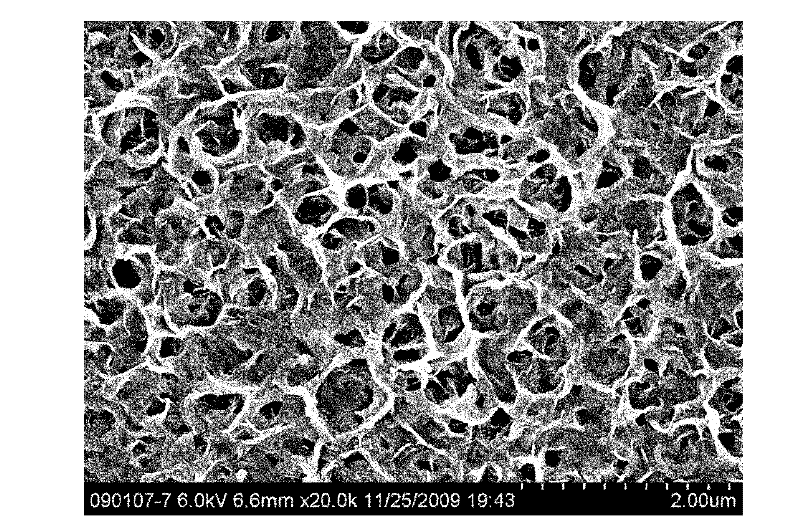
[0049] (2) Reaction step: the ITO glass substrate that step (1) system has metal indium thin film (thickness is 30 nanometers) is put into the polytetrafluoroethylene liner of reactor, adds sulfur powder, and sulfur powder concentration is 0.0015 g / ml, then add anhydrous ethanol solvent to the height of 75% of the container, and at the same time put the polytetrafluoroethylene liner into the stainless steel jacket and place it in a constant temperature blast drying oven with a temperature programming function, and raise the temperature to 180°C for reaction 24 hours.

[0050] (3) Post-processing: after the reaction, close the constant temperature blast drying oven and cool down to room temperature naturally. After washing the product with deionized water and absolute ethanol in sequence, the sample was dried in a vacuum drying oven at a constant temperature of 50° C. for 1 hour. Finally, the obtained indium sulfide film sample...

Embodiment 3

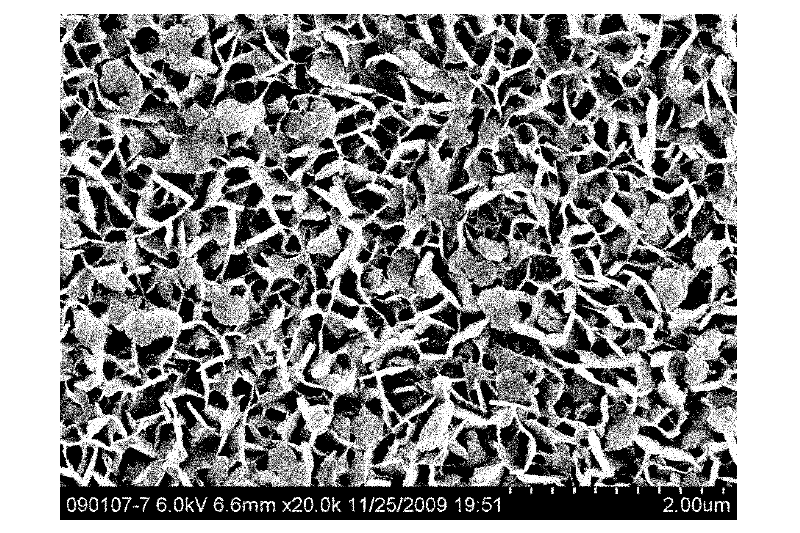
[0052] (1) preparatory work: with embodiment 1

[0053](2) Reaction step: the ITO glass substrate that step (1) system has metal indium thin film (thickness is 40 nanometers) is put into the polytetrafluoroethylene liner of reactor, adds sulfur powder, and sulfur powder concentration is 0.001 g / ml, then add anhydrous ethanol solvent to the height of 75% of the container, and at the same time put the polytetrafluoroethylene liner into the stainless steel jacket and place it in a constant temperature blast drying oven with a temperature-programming function, and raise the temperature to 180°C for reaction 12 hours.

[0054] (3) Post-processing: after the reaction, close the constant temperature blast drying oven and cool down to room temperature naturally. After washing the product with deionized water and absolute ethanol in sequence, the sample was dried in a vacuum drying oven at a constant temperature of 50° C. for 1 hour. Finally, the obtained indium sulfide film sample w...


PUM

PropertyMeasurementUnit
thicknessaaaaaaaaaa
thicknessaaaaaaaaaa
thicknessaaaaaaaaaa

Abstract

The invention relates to a solar cell device based on an In2S3 netted nanocrystal array and a P3HT hybrid film. The device is produced as follows: first, producing a netted indium sulfide nanocrystal array by reaction in situ on ITO glass having a nano-indium surface, and then compositing the netted indium sulfide nanocrystal array with P3HT to assemble the film solar cell device. The preparationmethod comprises the following steps of: putting the ITO substrate material having a nano-indium surface, elemental sulfur powder and anhydrous ethanol solvent into a reaction kettle, directly reacting for 12 to 14 hours under temperature of between 140 DEG C and 180 DEG C to obtain a nano netted indium sulfide nanocrystal array film at the surface of the ITO substrate material by reaction in situ; after the reaction, naturally cooling to room temperature; successively cleaning end products with deionized water and anhydrous ethanol, and drying in vacuum under 50 DEG C; then spinningly coating P3HT on the prepared indium sulfide film under argon protection, finally coating a layer of Al or Au electrode by vaporization to assemble the solar cell device. The method is low in cost and is environment friendly. Besides, compared with physical vaporous deposition, spray painting and splitting decomposition method and thermal evaporation, the method overcomes the shortage of complex preparation process.

Description

Technical field: [0001] The invention belongs to the technical field of optoelectronic materials, in particular to an in-situ preparation of In 2 S 3 A method of hybridizing thin films with P3HT mesh and assembling them into solar cell devices. Background technique: [0002] Inorganic nanocrystal-conjugated polymer solid thin film solar cell is a new type of heterojunction photovoltaic cell that uses semiconductor nanocrystals as electron acceptors and conjugated polymers as electron donors. High, good chemical stability, especially some nanocrystals such as sulfur and selenide of transition metals have strong absorption characteristics in the near infrared, and retain the good flexibility and processability of polymer materials. At present, the inorganic nanocrystals that have been studied more include CdSe, CdS, ZnS and so on. Among the conjugated polymers, the field-effect mobility of P3HT (polymer of 3-hexylthiophene) is the highest, reaching 0.1 cm 2 ·V -1 ·s -1 ....

Claims


Application Information

Patent Timeline
Patent Type & Authority Patents(China)
IPC IPC(8): H01L51/42H01L51/46H01L51/48
CPCY02E10/50Y02E10/549
Inventor 郑直贾会敏何伟伟陈雪武赵红晓雷岩李品将张翼东李静杨风岭
Owner XUCHANG UNIV
Why Eureka
Try Eureka