Step-like groove-grid high electron mobility transistor

A high electron mobility, transistor technology, applied in the field of microelectronics, can solve the problems of complex transistor fabrication process and increase the difficulty of devices, and achieve the effect of reducing source-drain contact resistance, improving device performance, and being easy to implement.

Inactive Publication Date: 2011-07-20
XIDIAN UNIV
View PDF6 Cites 36 Cited by
  • Summary
  • Abstract
  • Description
  • Claims
  • Application Information

AI Technical Summary

Problems solved by technology

However, the manufacturing process of high electron mobility transistors with stepped field plate and multilayer field plate structure is relatively complicated, and each additional layer of field plate requires additional process steps such as photolithography, metal deposition, dielectric material deposition, stripping, and cleaning. , and to make the insulating dielectric material deposited under the field plates of each layer have an appropriate thickness, multiple process adjustments must be carried out, which greatly increases the difficulty of device manufacturing

Method used


Image

  • Step-like groove-grid high electron mobility transistor
  • Step-like groove-grid high electron mobility transistor
  • Step-like groove-grid high electron mobility transistor

Examples


Embodiment 1

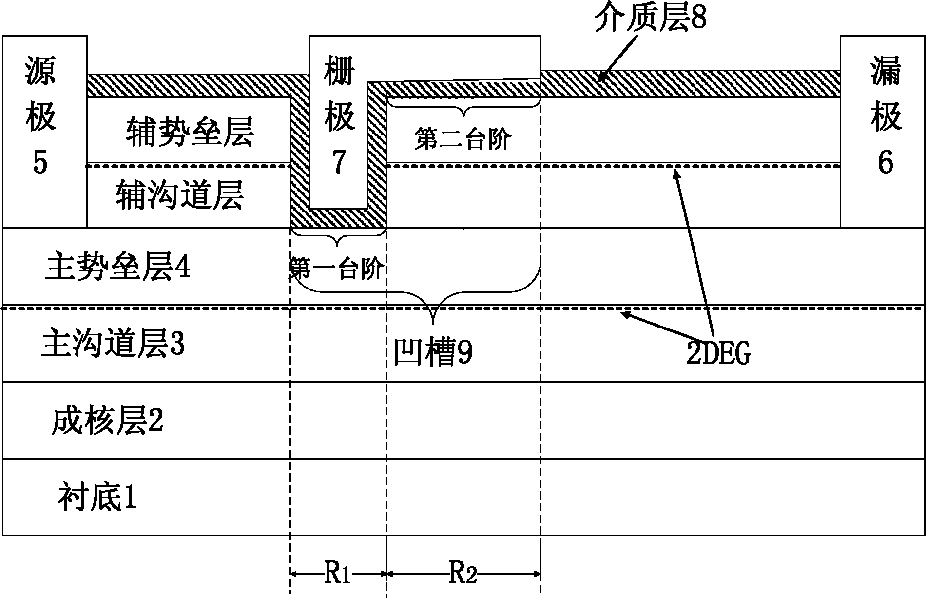
[0041] see figure 1 , the structure of the step type groove gate high electron mobility transistor HEMT of the present invention is: above the substrate 1 is the nucleation layer 2; above the nucleation layer 2 is the main channel layer 3; above the main channel layer 3 is the main potential Barrier layer 4, a two-dimensional electron gas 2DEG is formed on the interface between the main channel layer 3 and the main barrier layer 4; the source electrode 5 and the drain electrode 6 are on both sides of the top of the main barrier layer 4, and the gate 7 is in the middle; An auxiliary channel layer and an auxiliary barrier layer are sequentially added to the barrier layer 4, and 2DEG is formed on the interface between the auxiliary channel layer and the auxiliary barrier layer; a dielectric layer 8 is arranged above the auxiliary barrier layer; the auxiliary barrier layer There is a groove 9 between the main barrier layer 4, the depth of the groove decreases stepwise, the first s...

Embodiment 2

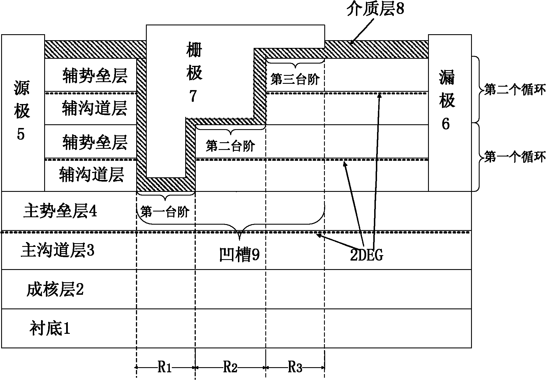
[0043] see figure 2 , the structure of the step type groove gate high electron mobility transistor HEMT of the present invention is: above the substrate 1 is the nucleation layer 2; above the nucleation layer 2 is the main channel layer 3; above the main channel layer 3 is the main potential Barrier layer 4, a two-dimensional electron gas 2DEG is formed on the interface between the main channel layer 3 and the main barrier layer 4; the source electrode 5 and the drain electrode 6 are on both sides of the top of the main barrier layer 4, and the gate 7 is in the middle; The barrier layer 4 is sequentially increased with an alternating cycle heterostructure composed of two auxiliary channel layers and auxiliary barrier layers, wherein a 2DEG is formed on the interface between each auxiliary channel layer and the auxiliary barrier layer immediately above it. ; There is a dielectric layer 8 above the top auxiliary barrier layer; a groove 9 is provided between the auxiliary barrie...

Embodiment 3

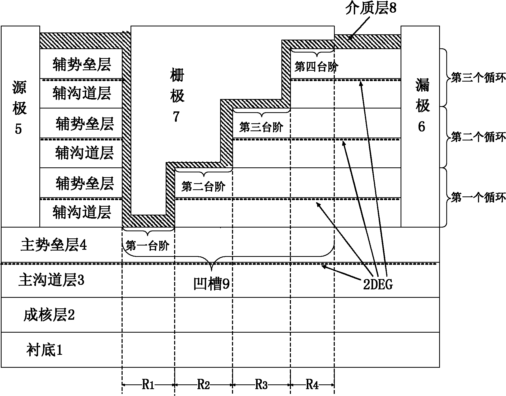
[0045] see image 3 , the structure of the step type groove gate high electron mobility transistor HEMT of the present invention is: above the substrate 1 is the nucleation layer 2; above the nucleation layer 2 is the main channel layer 3; above the main channel layer 3 is the main potential Barrier layer 4, a two-dimensional electron gas 2DEG is formed on the interface between the main channel layer 3 and the main barrier layer 4; the source electrode 5 and the drain electrode 6 are on both sides of the top of the main barrier layer 4, and the gate 7 is in the middle; An alternating cycle heterostructure composed of three auxiliary channel layers and auxiliary barrier layers is sequentially added to the barrier layer 4, wherein 2DEG is formed on the interface between each auxiliary channel layer and the auxiliary barrier layer immediately above it; There is a dielectric layer 8 above the top auxiliary barrier layer; a groove 9 is provided between the auxiliary barrier layer a...


PUM


Abstract

The invention discloses a step-like groove-grid high electron mobility transistor, mainly solving the problems of low breakdown voltage and complex field-plate manufacturing process in the prior art. The step-like groove-grid high electron mobility transistor comprises a substrate (1), a nucleating layer (2), a main channel layer (3) and a main barrier layer (4) from the bottom up, wherein a source electrode (5) and a drain electrode (6) are arranged on two side of the top end of the main barrier layer (4), a grid electrode (7) is arranged in the middle of the top end of the main barrier layer (4), and the main barrier layer (4) is provided with n alternate-circulation heterostructures formed by auxiliary channel layers and auxiliary barrier layers, wherein n ranges from 1 to 3; and a groove (9) is arranged between a topmost auxiliary barrier layer and the main barrler layer (4), and the wall of the groove, adjacent to a drain electrode side, is step-like; and the grid electrode (7) is arranged in the groove (9), and a dielectric layer (8) is arranged between the grid electrode and the groove. In the invention, the breakdown voltage is improved, the ohmic contact resistance between the source electrode and the drain electrode is decreased, the process is simple, and the step-like groove-grid high electron mobility transistor can be used a high-temperature and high-frequency high-power device with high reliability.

Description

technical field [0001] The invention belongs to the technical field of microelectronics and relates to semiconductor devices. Specifically, it is a stepped groove gate high electron mobility transistor HEMT, which can be used as a high-temperature, high-frequency, high-reliability, and high-power device. technical background [0002] Power semiconductor devices have been widely used in many power fields such as switching power supplies, automotive electronics, industrial control, and radio communications. As a typical representative of wide bandgap semiconductor materials, GaN-based materials have the characteristics of large bandgap width, high electron saturation drift velocity, high breakdown field strength and good thermal conductivity, and can be used to make high-temperature, high-frequency and high-power electronic devices. [0003] With the in-depth research on GaN-based HEMTs, it is found that when the high electron mobility transistor is working, the electric fiel...

Claims


Application Information

Patent Timeline
Patent Type & Authority Applications(China)
IPC IPC(8): H01L29/778H01L29/06H01L29/205H01L29/423H01L21/335H01L21/285
Inventor 张进成付小凡郝跃马晓华王冲陈珂奚鹏程解露李亮薛晓咏
Owner XIDIAN UNIV
Why Eureka
Try Eureka