Method for manufacturing three-dimensional nano grid structure based on one-dimensional soft template nanoimprinting

A nanoimprinting and three-dimensional nanotechnology, which is applied in the field of manufacturing three-dimensional nanogrid structures based on one-dimensional soft template nanoimprinting technology, can solve the problems of increasing the production cost of nanostructures, shortening the service life of templates, and damage to hard templates. Reduce production difficulty, reduce processing cost, and reduce production cost

Inactive Publication Date: 2011-07-27
DALIAN UNIV OF TECH
View PDF4 Cites 10 Cited by
  • Summary
  • Abstract
  • Description
  • Claims
  • Application Information

AI Technical Summary

Problems solved by technology

They all use hard templates for imprinting, which may cause permanent damage to the hard template

Method used


Image

  • Method for manufacturing three-dimensional nano grid structure based on one-dimensional soft template nanoimprinting
  • Method for manufacturing three-dimensional nano grid structure based on one-dimensional soft template nanoimprinting
  • Method for manufacturing three-dimensional nano grid structure based on one-dimensional soft template nanoimprinting

Examples


Embodiment 1

[0031] Embodiment 1: Making a three-dimensional nanogrid structure with Sub-25nm rectangular nano-dots

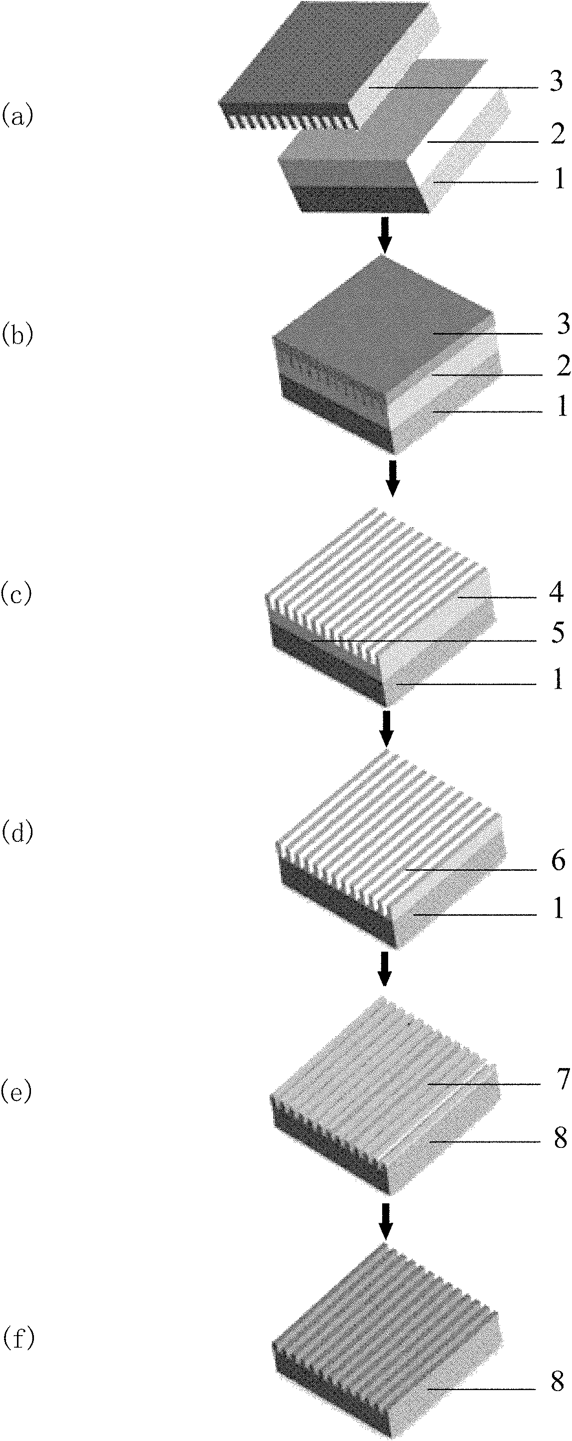
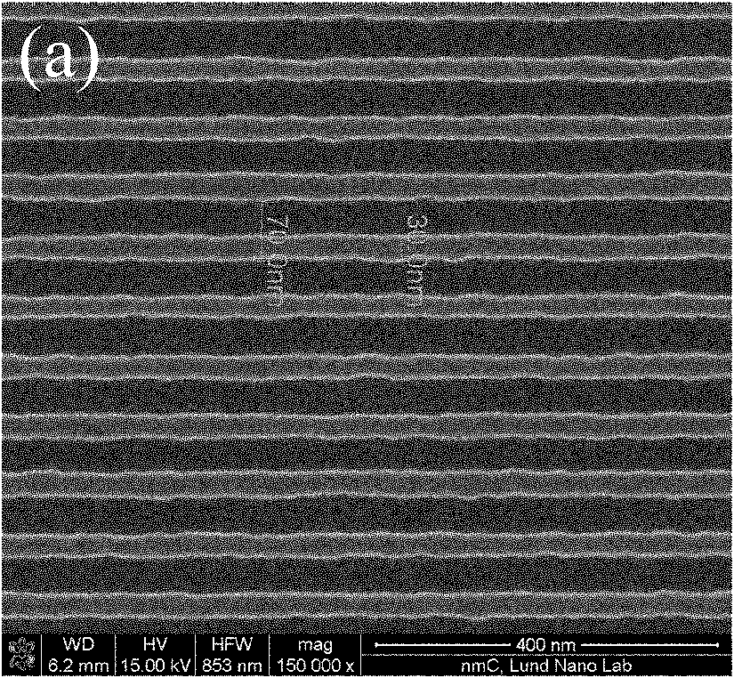
[0032] Prepare the soft template 3 first, on which there is a one-dimensional nano-grating structure, the pattern area is 6mm×10mm, the grating period is 70nm, the line width is 40nm, and the height is 50nm. Figure 2 is the SEM photograph of the master template and the replicated soft template, the soft template material is a fluoropolymer. Take a 2-inch silicon wafer as a substrate 1, clean it, and then spin-coat a thermoplastic UV-curable nano-imprint adhesive 2. The thickness of the embossing glue 2 is between 30-50nm. as attached figure 1 As shown in (b), the soft template was used to imprint on the substrate spin-coated with imprinting glue. The imprinting pressure was 20 bar, the imprinting temperature was 65°C, the imprinting time was 180s, and then exposed to ultraviolet light for 30s. as attached figure 1 As shown in (c), the soft template is separated from the...

Embodiment 2

[0046] Embodiment 2: Making a three-dimensional nanogrid structure with Sub-25nm diamond-shaped nano-dots

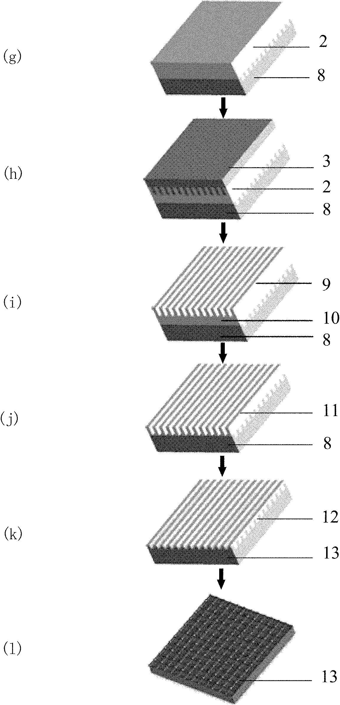
[0047] Using the same soft template as in Example 1, the same embossing and etching parameters, by adjusting the angle between the direction of the grating lines on the soft template 3 and the direction of the grating lines on the imprinting substrate 8 in the second imprinting process to be 45° , the line width of the obtained three-dimensional silicon nanogrid structure is 25nm, the period is 70nm, and the nano-dot size at the top of the intersection of the two gratings is sub-25nm. The shapes of the nanogrid structure and the nanodots are rhombuses with an included angle of 45°.


PUM


Abstract

The invention belongs to the technical field of micro-nano manufacturing, and in particular relates to a method for manufacturing a large-area three-dimensional nano grid structure based on a one-dimensional soft template nanoimprinting technology. The method comprises the following steps of: performing first-time nanoimprinting by using a soft template; removing a imprinting glue residual layer by oxygen reactive ion etching (RIE); degumming by using a manufactured imprinting glue pattern as a masking film etching substrate material to obtain a one-dimensional nano grating structure; performing a second-time imprinting and etching process by using parameters the same as those of the previous imprinting and etching process; and adjusting the included angle formed between the direction of the template during the second-time imprinting and the direction of the template during the first-time imprinting to be between 0 and 90 degrees so as to obtain the three-dimensional nano grid structure with a 25nm nano-point. Due to the adoption of the soft template, permanent damages caused by contacting a hard template with a hard substrate can be effectively avoided, and the usage of a three-dimensional template is avoided simultaneously. The size and the shape of the manufactured nano structure are controllable. The method is low in cost and high in efficiency, controllability and resolution.

Description

technical field [0001] The invention belongs to the technical field of micro-nano manufacturing, and relates to a method for manufacturing a three-dimensional nano-grid structure based on a one-dimensional soft template nano-imprinting technology. Background technique [0002] Three-dimensional nanostructures have broad application prospects in MEMS / NEMS, micro / nanofluidic devices, photonic crystals, display technology, diffractive optics and other fields. In terms of three-dimensional nanostructure fabrication technology, researchers have explored a variety of lithography techniques, including electron beam direct writing technology, focused ion beam lithography technology, X-ray lithography technology, and nanoimprint technology. Schleunitz et al. of the Paul Scherrer Institute in Switzerland used a process of controlling the exposure dose of electron beams in different exposure areas, combined with thermal reflow technology to produce a three-dimensional nanoimprint templ...

Claims


Application Information

Patent Timeline
IPC IPC(8): G03F7/00
Inventor 褚金奎孟凡涛王志文韩志涛
Owner DALIAN UNIV OF TECH
Why Eureka
Try Eureka