Light-emitting element and manufacturing method and light-emitting method thereof
A light-emitting element and manufacturing method technology, applied in the direction of electrical components, cold cathode manufacturing, electrode system manufacturing, etc., can solve problems such as low luminous efficiency and limiting the application of field emission devices
- Summary
- Abstract
- Description
- Claims
- Application Information
AI Technical Summary
Problems solved by technology
Method used
Image
Examples
Embodiment 1
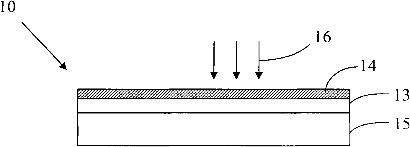
[0043] Choose a size of 1×1cm 2 Double-sided polished quartz substrate, using magnetron sputtering method to form Y-containing substrate on the substrate 1.94 Tb 0.06 SiO 5 Light-emitting film, and then use magnetron sputtering equipment to deposit a metal silver layer with a thickness of 2 nanometers on the surface of the light-emitting film, and then place it in a vacuum degree of less than 1×10 -3 In a Pa vacuum environment, annealing is performed at a temperature of 300° C. for half an hour, and then cooled to room temperature to obtain the desired yttrium silicate terbium-doped light-emitting element. Such as figure 1 Shown is a structural diagram of a light-emitting element doped with yttrium silicate and terbium, wherein the substrate 15 is a quartz substrate, and the light-emitting film 13 is a prepared Y 1.94 Tb 0.06 SiO 5 The metal layer 14 is a 2 nanometer silver layer. The electron beam 16 emitted by the electron gun directly hits the metal layer 14. The electron beam ...
Embodiment 2
[0047] Choose a size of 1×1cm 2 Double-sided polished quartz substrate, using electron beam evaporation method to prepare Y on the substrate 1.998 Tb 0.002 SiO 5 Use magnetron sputtering equipment to deposit a metal gold layer with a thickness of 0.5 nanometers on the surface of the light-emitting film, and then place it in a vacuum less than 1×10 -3 In a Pa vacuum environment, annealing was performed at a temperature of 200° C. for 1 hour, and then cooled to room temperature to obtain the yttrium silicate terbium-doped light-emitting element of this example.
Embodiment 3
[0049] Choose a size of 1×1cm 2 Double-sided polished sapphire substrate, using chemical vapor deposition method to form Y on the substrate 1.995 Tb 0.005 SiO 5 Use magnetron sputtering equipment to deposit a metal aluminum layer with a thickness of 200 nanometers on the surface of the light-emitting film, and then place it in a vacuum less than 1×10 -3 In a Pa vacuum environment, annealing was performed at a temperature of 500° C. for 5 hours and then cooled to room temperature to obtain the yttrium silicate terbium-doped light-emitting element of this example.
PUM
| Property | Measurement | Unit |
|---|---|---|
| Thickness | aaaaa | aaaaa |
Abstract
Description
Claims
Application Information
 - R&D
- Intellectual Property
- Life Sciences
- Materials
- Tech Scout
- Unparalleled Data Quality
- Higher Quality Content
- 60% Fewer Hallucinations
Browse by: Latest US Patents, China's latest patents, Technical Efficacy Thesaurus, Application Domain, Technology Topic, Popular Technical Reports.
© 2025 PatSnap. All rights reserved.Legal|Privacy policy|Modern Slavery Act Transparency Statement|Sitemap|About US| Contact US: help@patsnap.com


