LED encapsulation structure
A technology of LED packaging and LED chips, which is applied to semiconductor devices, electrical components, circuits, etc., and can solve problems such as rising operating temperature and loss of light efficiency of LED devices
- Summary
- Abstract
- Description
- Claims
- Application Information
AI Technical Summary
Problems solved by technology
Method used
Image
Examples
Embodiment Construction
[0016] In order to make the technical problems, technical solutions and beneficial effects to be solved by the present invention clearer, the present invention will be further described in detail below in conjunction with the accompanying drawings and embodiments. It should be understood that the specific embodiments described here are only used to explain the present invention, not to limit the present invention.
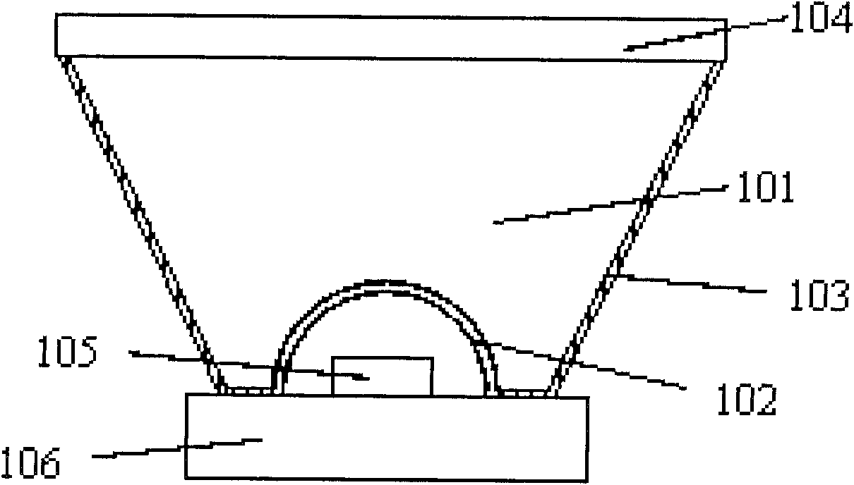
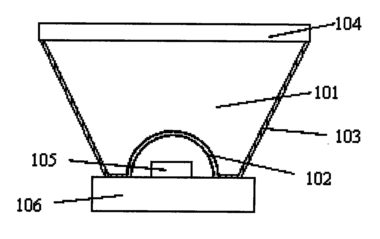
[0017] Please refer to figure 1 , is a preferred embodiment of the LED package structure of the present invention, the LED package structure includes a base 106, an LED chip 105 on the base 106, an optical lens 101, and a second optical lens on the light incident surface of the optical lens 101. An optical film layer 102, and a phosphor layer 104 located on the light-emitting surface of the optical lens 101, the first optical film layer 102 is concave. The first optical film layer 102 is formed by alternate coating of two materials with different refractive indice...
PUM
 Abstract
Description
Claims
Application Information

