CDM (Charged Device Model) ESD (Electro-Static Discharge) protection circuit

An ESD protection and circuit protection technology, applied in the direction of emergency protection circuit devices, circuits, circuit devices, etc., can solve the problems of short time, damage, and easy breakdown of gate oxide, and achieve the effect of good performance and stable circuit.

Active Publication Date: 2011-08-10
SHANGHAI HUAHONG GRACE SEMICON MFG CORP
View PDF11 Cites 17 Cited by
  • Summary
  • Abstract
  • Description
  • Claims
  • Application Information

AI Technical Summary

Problems solved by technology

figure 1 It is a schematic diagram of an existing CDM ESD protection circuit and a protected functional unit, figure 2 for figure 1 The schematic cross-section of the circuit shown, as figure 1 and figure 2 As shown, the existing CDM ESD protection circuit is implemented by the ESD protection unit 101 (such as a MOS transistor), but with the reduction of the process size, the gate oxide of the MOS transistor of the functional unit is getting thinner and thinner. The functional unit 102 is provided with a discharge channel for the substrate, but because the voltage of the ESD is too high and the time is too short, the gate oxide of the MOS transistor of the functional unit 102 is very easily broken down (for example figure 2 The discharge current shown in I ESD ), so that the functional unit is damaged
[0006] In order to find a better solution, the US Patent No. US6885529B2 discloses a CDM ESD structure that uses a deep well structure to solve the threat of CDM, although this can make the functional units in the isolated N well, thereby greatly reducing the number of functional units The electrostatic charge in the P-well region where it is located, but although the amount of charge is reduced, it can still break down the gate oxide layer of the functional unit MOS transistor and destroy it

Method used


Image

  • CDM (Charged Device Model) ESD (Electro-Static Discharge) protection circuit
  • CDM (Charged Device Model) ESD (Electro-Static Discharge) protection circuit
  • CDM (Charged Device Model) ESD (Electro-Static Discharge) protection circuit

Examples


no. 1 example

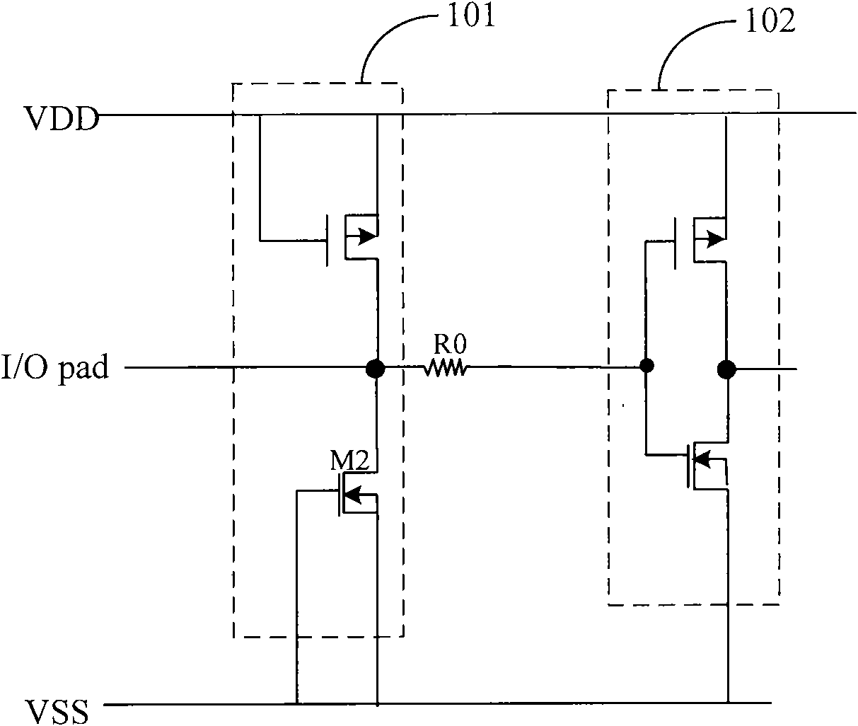
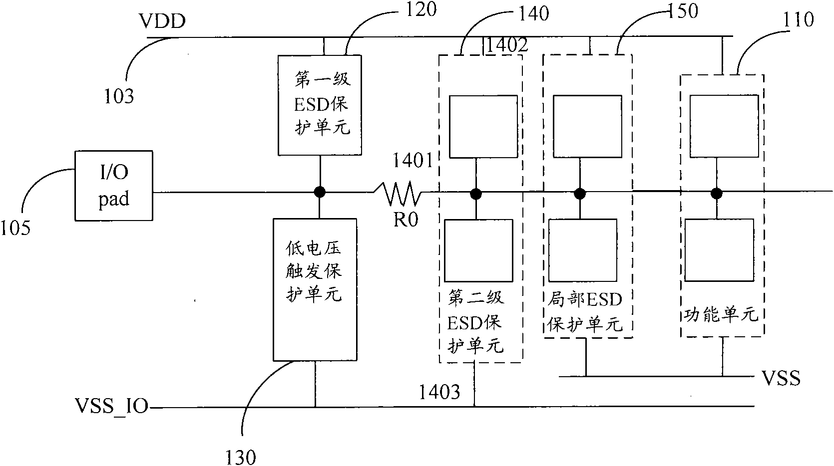
[0060] image 3 It is a schematic diagram of a CDM ESD protection circuit and a protected functional unit according to an embodiment of the present invention. Combine below image 3 The CDM ESD protection circuit of the embodiment of the present invention is described, image 3 It mainly includes: power line 103 (input voltage is VDD), substrate Sub and input / output pin (I / Opad) 105, functional unit 110, first-level ESD protection unit 120, low-voltage trigger protection unit 130, second level ESD protection unit 140 and localized ESD protection unit 150 .

[0061] Wherein, the functional unit 110 is coupled to the input / output pin (I / Opad) 105 through a resistor R0, and the functional unit 110 is a core unit of the CDM ESD protection circuit, and is used to realize the function of the circuit.

[0062] The first end of the first-level ESD protection unit 120 is coupled to the input / output pin 105, and the second end is coupled to the power line 103. When the potential of t...

no. 2 example

[0092] Figure 6 It is a schematic diagram of a CDM ESD protection circuit according to the second embodiment of the present invention. Combine below Figure 6 The CDM ESD protection circuit of the second embodiment of the present invention will be described, and the similarities with the first embodiment will not be repeated, and the difference lies in:

[0093] In this embodiment, the SCR includes:

[0094] a capacitor, the first end of which is coupled to the input and output pins, and the second end is coupled to the first node;

[0095] A first resistor R1, whose first end is coupled to the substrate, and whose second end is coupled to the first node 10; NMOS transistor M11, whose gate is coupled to the first node 10, and whose source is coupled to the substrate Sub; PNP transistor P1, the emitter of which is coupled to the input / output pin 105, the base is coupled to the drain of the NMOS transistor M11, and the collector is coupled to the second node 20; NPN transist...


PUM


Abstract

The invention provides a CDM (Charged Device Model) ESD (Electro-Static Discharge) protection circuit which is used for protecting a functional unit. The CDM ESD protection circuit comprises a first stage of ESD protection unit, a low voltage trigger protection unit, a second stage of ESD protection unit and a local ESD protection unit, wherein the first end of the low voltage trigger protection unit is coupled to the input / output pin, and the second end of the low voltage trigger protection unit is coupled to the substrate. When the electric potential of the substrate is smaller than that of the input / output pin and exceeds a second specific voltage, the low voltage trigger protection unit operates. Therefore, the performance of the CDM ESD protection circuit is improved.

Description

technical field [0001] The invention relates to an electrostatic discharge (ESD) circuit, in particular to a CDM ESD protection circuit. Background technique [0002] Integrated circuits (ICs) are prone to destructive electrostatic discharge (ESD) during manufacturing, assembly and testing or in final applications, so that integrated circuits are damaged by static electricity. [0003] ESD is typically produced by the discharge of a high voltage potential (eg, several thousand volts) and results in a short duration (eg, 100 ns) pulse of high current. ESD is usually divided into three categories. The first category is caused by the contact between human and IC. Usually, HBM (human body model) type ESD protection circuit can be made for this type of ESD. The second category is caused by the contact between mechanical equipment and IC. Generally, MM (machine model) type ESD protection circuits can be made for this type of ESD; the third type is caused by the charging of the IC...

Claims


Application Information

Patent Timeline
IPC IPC(8): H02H9/04H01L23/60
Inventor 单毅唐成琼
Owner SHANGHAI HUAHONG GRACE SEMICON MFG CORP
Why Eureka
Try Eureka