Process for producing conducting circuit of capacitive touch screen

A technology of capacitive touch screen and conductive circuit, which is applied in the field of manufacturing printed circuits, can solve problems such as burrs, high cost, and high price of capacitive touch screen, and achieve the effect of improving production efficiency and good fluency

Inactive Publication Date: 2011-08-17
EELY ECW TECH
View PDF3 Cites 7 Cited by
  • Summary
  • Abstract
  • Description
  • Claims
  • Application Information

AI Technical Summary

Problems solved by technology

The cost of these processes is high, resulting in expensive capacitive touch screens
In order to solve this problem, the currently commonly used method is to use screen printing conductive silver glue on the ITO film, such as the Chinese patent application number 200910109340.7, although the production cost is reduced, but there are the following defects: (1) due to the conductive silver glue It has penetrating effect, and it is very difficult to print fine line silver glue, and the minimum can only print conductive lines with a line width and line spacing of 80×80μm; (2) it is easy to appear burrs and jagged phenomena when printing lines; (3) it is easy to print when printing The dry board phenomenon leads to the inability to continue production
The above production process problems have always been the bottleneck hindering the development of the industry

Method used


Image

  • Process for producing conducting circuit of capacitive touch screen
  • Process for producing conducting circuit of capacitive touch screen

Examples


Embodiment 1

[0021] (1) Making Cu conductive lines:

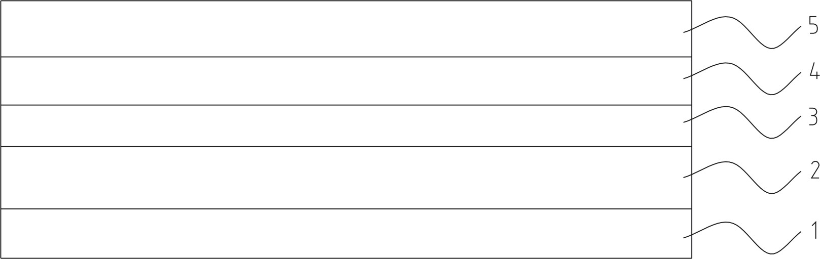
[0022] a. Attach the ITO-Cu film on the substrate, and use a film laminating machine to attach the photosensitive dry film (the photosensitive dry film used in this example is LAMINAR E9500, with a thickness of 30 μm) to the surface of the Cu layer 5 of the ITO-Cu film , where the lamination temperature is 110°C, the lamination speed is 1.0m / min, and the lamination pressure is 0.3 MPa. Under the irradiation of 4000W UV light, the photosensitive dry film on the surface of the Cu layer 5 is exposed by using a film with a Cu conductive circuit pattern, and the exposure time is 10s. Then use the development process line to rinse and develop the unexposed photosensitive dry film part, the development temperature is 25 °C, and the spray pressure of the developer is 20kg / cm 2 , The material conveying speed during developing is 2.0m / min. After development, the ITO-Cu film is covered with a shielding photosensitive dry film consistent with the...

Embodiment 2

[0033] The difference from Example 1 is that in step (a), the thickness of the photosensitive dry film used is 15 μm, and a thinner Cu conductive circuit can be fabricated.

Embodiment 3

[0035] Different from Example 1, in step (b), the ratio of each component of the Cu stripping solution used is (by weight percentage): CuCl 2 8%, ethanol ammonia 10%, NaCl 2%, sodium citrate 0.05%, and the rest is water.


PUM


Abstract

The invention discloses a process for producing a conducting circuit of a capacitive touch screen. The method comprises the following steps of: (1) adhering a photosensitive dry film to the surface of a Cu layer of an ITO-Cu (Indium Tin Oxide-Copper) film, exposing, curing the photosensitive dry film corresponding to a Cu conducting circuit pattern, removing uncured photosensitive dry film and removing the Cu layer which is not covered by the photosensitive dry film to obtain a Cu conducting circuit; (2) forming an ITO conducting circuit pattern on the surface of an ITO layer, which is not covered by the Cu layer, of the ITO-Cu film from the ink in a screen printing mode, drying the ink, and removing the ITO layer which is not covered by the Cu layer and the ink to obtain an ITO conducting circuit; and (3) removing shielding ink on the Cu layer and the ITO layer. By adopting the method for manufacturing the conducting circuit of the capacitive touch screen, the manufactured Cu conducting circuit is finer, has higher smoothness, does not have burr and saw-tooth phenomena and can be continuously produced.

Description

technical field [0001] The invention relates to a method for manufacturing a printed circuit, in particular to a production process for a conductive circuit of a capacitive touch screen. Background technique [0002] Touch screens include resistive, capacitive, infrared and surface acoustic wave touch screens. Among them, capacitive touch screen technology has developed into a multi-touch that can recognize its surface, which is convenient for users to easily realize various complex operations on files and games through simple actions. It has multi-touch function and has attracted widespread attention. The realization principle of the multi-touch function of the capacitive touch screen is generally to partition the ITO film of the touch screen and design it into a specific shape, and then the touch screen controller performs capacitance inspection and control on each independent ITO film with a specific shape Multi-touch on their surfaces. In order to electrically connect ...

Claims


Application Information

Patent Timeline
Patent Type & Authority Applications(China)
IPC IPC(8): G06F3/044
Inventor 白震勇王雪镅
Owner EELY ECW TECH
Why Eureka
Try Eureka