Semiconductor structure and manufacturing method thereof

A technology of semiconductor and interconnect structure, applied in the direction of semiconductor/solid-state device manufacturing, semiconductor devices, semiconductor/solid-state device components, etc., can solve the problems of affecting the fusing current and fusing time, uneven thickness of the fusing area, and difficult thickness. , to achieve the effect of easy fuse thickness, simple structure and easy control

Active Publication Date: 2011-08-17
SHANGHAI HUAHONG GRACE SEMICON MFG CORP
View PDF10 Cites 13 Cited by
  • Summary
  • Abstract
  • Description
  • Claims
  • Application Information

AI Technical Summary

Problems solved by technology

However, in the above two technologies, the metal layer is first deposited, then etched, and then the metal layer used as the fusing zone is thinned. This not only complicates the pr

Method used


Image

  • Semiconductor structure and manufacturing method thereof
  • Semiconductor structure and manufacturing method thereof
  • Semiconductor structure and manufacturing method thereof

Examples


Example Embodiment

[0048] In order to make the above objectives, features and advantages of the present invention more obvious and understandable, the specific embodiments of the present invention will be described in detail below with reference to the accompanying drawings.

[0049] In the following description, many specific details are set forth in order to fully understand the present invention, but the present invention can also be implemented in other ways different from those described herein, so the present invention is not limited by the specific embodiments disclosed below.
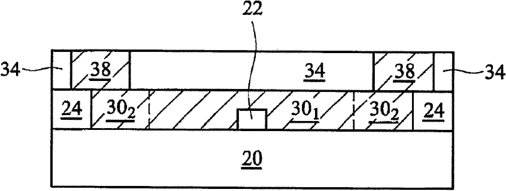
[0050] As described in the background art, in the prior art, in order to obtain a thinner fuse zone, a thinning process is required. This is not only a complicated process, but also the thickness of the fuse zone after the thinning process is uneven and its thickness is not easy to accurately control , Thereby affecting the fusing current and fusing time.

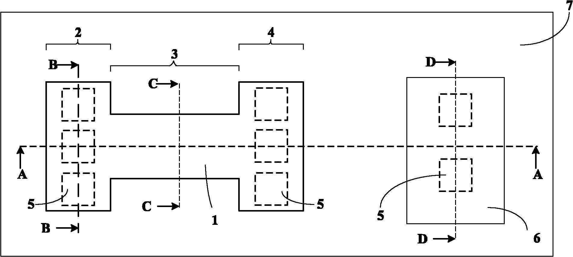
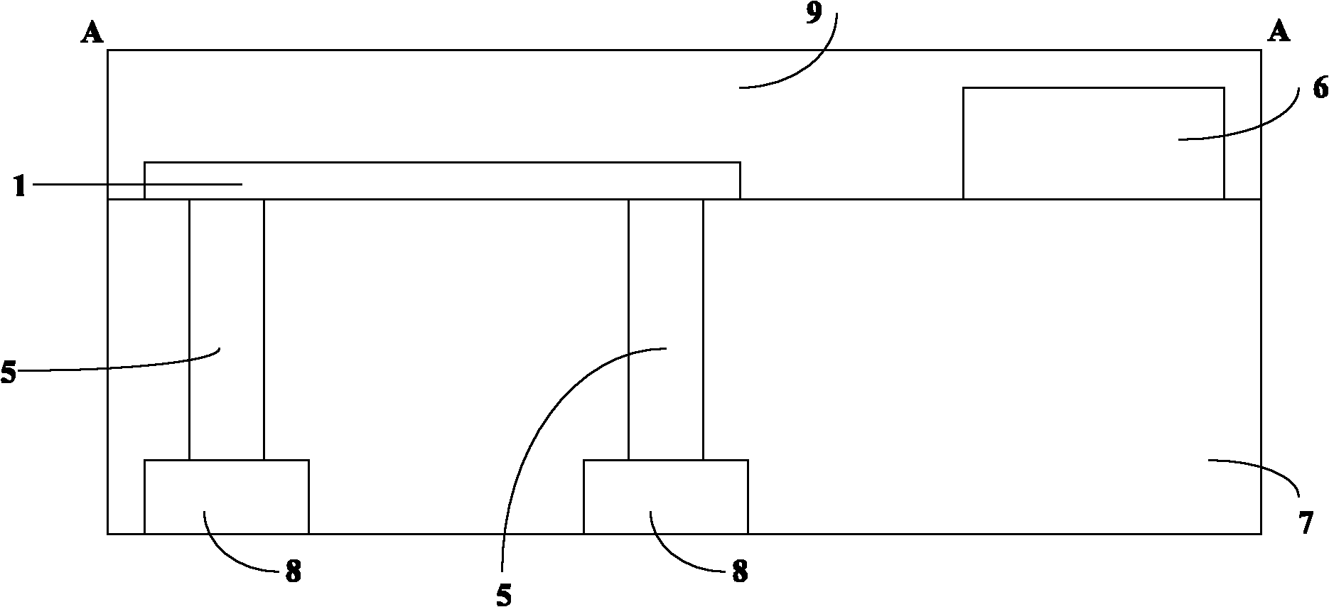
[0051] The present invention provides a semiconductor structure ...


PUM


Abstract

The invention provides a semiconductor structure and a manufacturing method thereof, belonging to the technical field of semiconductors. The structure comprises a substrate and one or more layers of interconnection structures, wherein the top layer of interconnection structure comprises a plurality of bottom metal wires, a plurality of contact plugs, an interlayer dielectric layer, a top metal wire, a metal fuse and an insulating layer. The metal fuse comprises a cathode, an anode and a fusing region, wherein the cathode is arranged on at least one residual contact plug, the anode is arranged on at least one residual contact plug, the contact plug below the cathode and the contact plug below the anode are arranged at different bottom metal wires, and the fusing region is respectively connected with the cathode and the anode. The semiconductor structure and the manufacturing method thereof disclosed by the invention are simple; through the manufacturing method disclosed by the invention, the thickness of the manufactured fuse by is easier to control and is thinner, thus the fuse can be fused by using low-energy laser or current.

Description

technical field [0001] The invention relates to a semiconductor structure and a preparation method thereof, in particular to a semiconductor structure including a fuse and a preparation method thereof. Background technique [0002] With the miniaturization and increase in complexity of the semiconductor process, semiconductor devices become more susceptible to various defects or impurities, and the failure of a single metal connection, diode or transistor often constitutes a defect of the entire chip. Therefore, in order to solve this problem, some fusible links (fusible links), that is, fuses (fuse), are formed in the integrated circuit in the prior art to ensure the availability of the integrated circuit. [0003] Generally speaking, fuses are used to connect redundant circuits in integrated circuits, and once the circuit is found to be defective, these connection lines can be used to repair or replace the defective circuit. In addition, the current fuse design also provi...

Claims


Application Information

Patent Timeline
IPC IPC(8): H01L23/525H01L23/522H01L21/768
Inventor 宗登刚彭树根李乐韦庆松
Owner SHANGHAI HUAHONG GRACE SEMICON MFG CORP
Why Eureka
Try Eureka