High-voltage LDMOS (landscape diffusion metal oxide semiconductor) device

A device and high-voltage technology, which is applied in the field of semiconductor high-voltage and low-resistance devices, can solve the problems of reduced reverse withstand voltage of LDMOS devices and the concentration cannot be made too high, and achieves the effect of improving reverse withstand voltage and reducing forward on-resistance.

Inactive Publication Date: 2011-08-17
UNIV OF ELECTRONICS SCI & TECH OF CHINA
View PDF3 Cites 15 Cited by
  • Summary
  • Abstract
  • Description
  • Claims
  • Application Information

AI Technical Summary

Problems solved by technology

Therefore, in order to ensure a certain withstand voltage, the length of the drift region 3 of the LDMOS device cannot be made too short; its concentration cannot be made too high, otherwise breakdown will occur near the PN junction of the well region 5 under the gate 9, causing The reverse withstand voltage of LDMOS devices is reduced

Method used


Image

  • High-voltage LDMOS (landscape diffusion metal oxide semiconductor) device
  • High-voltage LDMOS (landscape diffusion metal oxide semiconductor) device
  • High-voltage LDMOS (landscape diffusion metal oxide semiconductor) device

Examples


Embodiment 1

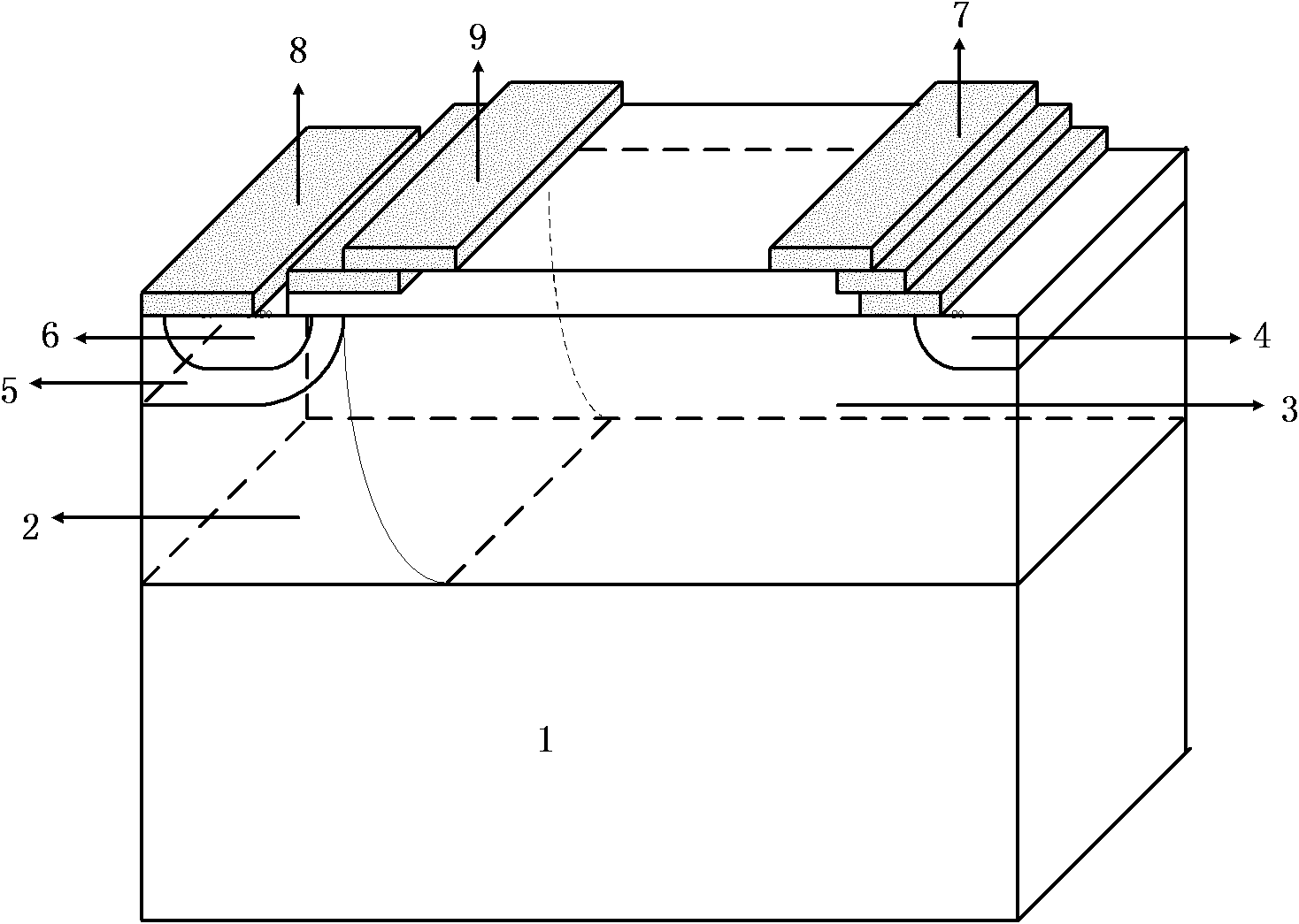
[0022] Embodiment one: if Figure 4 As shown, the LDMOS device includes a substrate 1, an epitaxial layer 2, a drift region 3, a drain region 4, a source region 6, a drain 7, a source 8, and a gate 9. In this embodiment, the LDMOS device is a P epitaxial N-channel LDMOS device, so the substrate 1 and the epitaxial layer 2 are p-type, and the drift region 3 is n - type, the drain region 4 and the source region 6 are n + type, the epitaxial layer 2 is located on the substrate 1, the drift region 3 is located on the side of the epitaxial layer 2 close to the drain region 4 and the lower surface spans the lower surface of the epitaxial layer 2, the drain region 4 and the source region 6 are located at both ends of the LDMOS device, There are two pairs of n-type semiconductor regions 10 and p-type semiconductor regions 11 alternately arranged across the lower surface of the epitaxial layer 2 on the interface between the substrate 1 and the epitaxial layer 2, the n-type semiconduct...

Embodiment 2

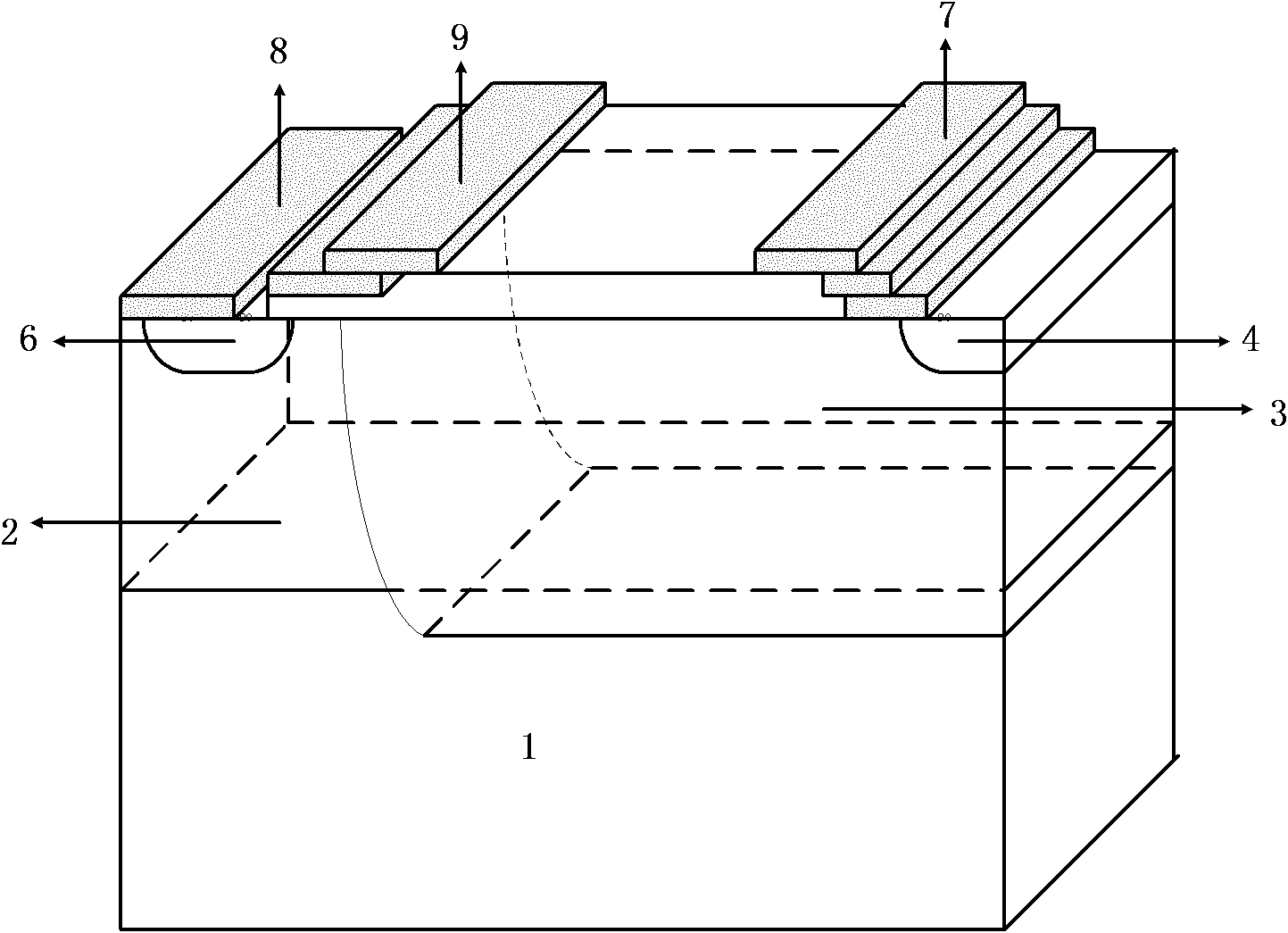
[0027] Embodiment two: if Figure 5 As shown, on the basis of Embodiment 1, in order to prevent the PN junction formed by the n-type semiconductor region 10 and the p-type semiconductor region 11 from affecting the electric field of the drain region 4, the length of the n-type semiconductor region 10 and the p-type semiconductor region 11 can be shortened To the interface between the drain region 4 toward the center and the drift region 3 .

Embodiment 3

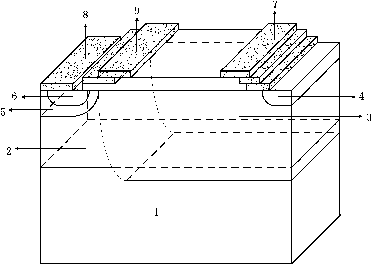
[0028] Embodiment three: as Figure 6 As shown, on the basis of Embodiment 1 or Embodiment 2, in order to prevent the n-type semiconductor region 10 and the p-type semiconductor region 11 from affecting the source region 6, the lengths of the n-type semiconductor region 10 and the p-type semiconductor region 11 can be adjusted to The shortening is not connected to the interface between the drift region 3 facing the source region 6 and the epitaxial layer 2 .


PUM


Abstract

The invention relates to a high-voltage LDMOS (landscape diffusion metal oxide semiconductor) device which comprises a substrate, an epitaxial layer, a drift region, a drain region, a source region and at least one pair of n-type semiconductor regions and p-type semiconductor regions, wherein the epitaxial layer is positioned above the substrate; the drift region is positioned on one side, close to the drain region, of the epitaxial layer, and the lower surface of the drift region is coincided with the lower surface of the epitaxial layer; the drain region and the source region are positioned at two ends of the LDMOS device; at least one pair of the n-type semiconductor regions and the p-type semiconductor regions are arrayed alternatively, pass through the lower surface of the epitaxial layer on the border surface of the substrate and the epitaxial layer; the border surface of the n-type semiconductor regions and the p-type semiconductor regions is in parallel with the surface voltage drop direction of a power device in working; and the n-type semiconductor regions and the p-type semiconductor regions are arrayed closely, thus a PN junction is formed. The invention has the beneficial effects that the n-type semiconductor regions and the p-type semiconductor regions provided by the invention are named a bulk reduced surface field layer, and the contradiction of improving the reverse withstand voltage and reducing the positive conduction resistance of the existing LDMOS device is solved effectively by the LDMOS device with the bulk reduced surface field layer.

Description

technical field [0001] The invention relates to semiconductor high-voltage and low-resistance devices in the field of electronic technology, in particular to high-voltage power devices manufactured on bulk silicon. Background technique [0002] With the rapid development of the semiconductor industry, PIC (Power Integrated Circuit, power integrated circuit) is continuously used in many fields, such as motor control, flat panel display drive control, computer peripheral drive control, etc., the PIC circuit used Among power devices, LDMOS (Lateral Double Diffused MOSFET, lateral double diffused metal oxide semiconductor field effect transistor) high-voltage devices have high operating voltage, simple process, and are easy to be compared with low-voltage CMOS (Complementary Metal Oxide Semiconductor, complementary metal oxide semiconductor) circuits. Compatibility in technology and other characteristics have attracted widespread attention. However, for semiconductor high-volta...

Claims


Application Information

Patent Timeline
Patent Type & Authority Applications(China)
IPC IPC(8): H01L29/78H01L29/06
CPCH01L29/0634H01L29/404H01L29/7835
Inventor 方健陈吕赟管超王泽华吴琼乐柏文斌杨毓俊黎俐
Owner UNIV OF ELECTRONICS SCI & TECH OF CHINA
Why Eureka
Try Eureka