Contact arrangement for establishing a spaced, electrically conducting connection between microstructured components

A contact device and micro-structuring technology, applied in the field of manufacturing such contact devices and component devices, can solve the problems of area loss and extra cost, and achieve the effect of small structure size

Inactive Publication Date: 2011-08-24
ROBERT BOSCH GMBH
View PDF1 Cites 5 Cited by
  • Summary
  • Abstract
  • Description
  • Claims
  • Application Information

AI Technical Summary

Problems solved by technology

However, this implies a considerable loss of area and thus additional costs

Method used


Image

  • Contact arrangement for establishing a spaced, electrically conducting connection between microstructured components
  • Contact arrangement for establishing a spaced, electrically conducting connection between microstructured components
  • Contact arrangement for establishing a spaced, electrically conducting connection between microstructured components

Examples


Embodiment Construction

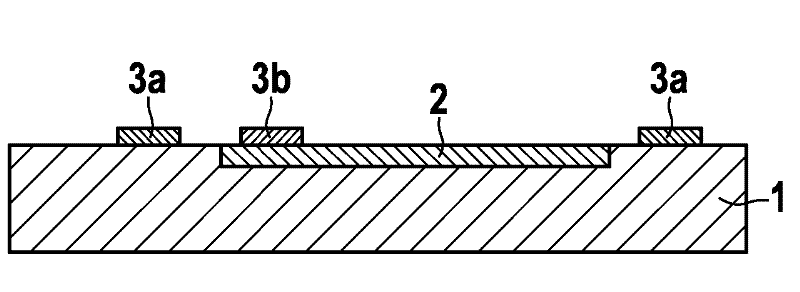
[0038] figure 1 A cap wafer 1 is shown, which comprises a microstructured first component 2 . Component 2 is shown schematically here and can be, for example, an application-specific integrated circuit (ASIC). The wafer 1 comprises a first contact device 3a and a second contact device 3b serving as a bonding frame. The first contacting device 3 a is mounted directly on the wafer, the second contacting device 3 b is mounted on the microstructured first component 2 .

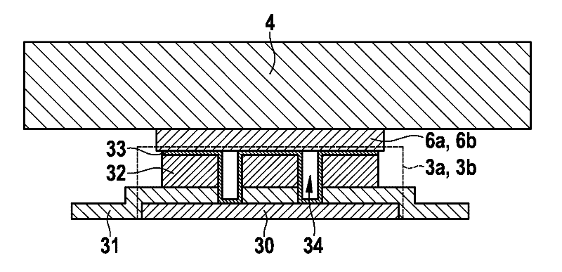
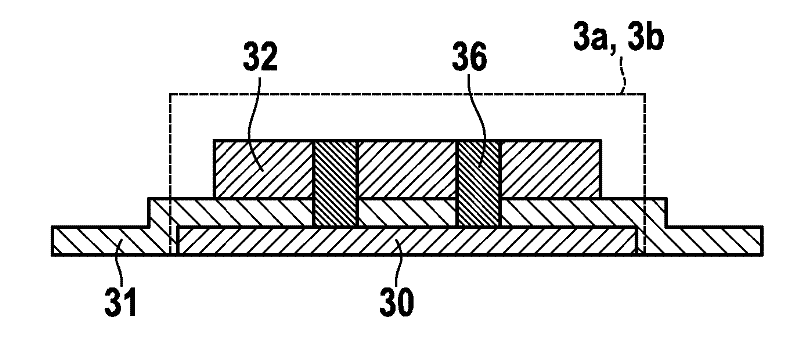
[0039] figure 2 A detailed view of the contacting devices 3a and 3b according to the invention is shown. In this case, the electrical connection contacts 30 are provided with a passivation layer 31 , wherein the material of the connection contacts 30 can be a metal such as aluminum or copper, which are used, for example, in ASICs as the uppermost wiring plane. Passivation layer 31 is typically a dielectric such as silicon dioxide or silicon nitride.

[0040] A dielectric spacer layer 32 is deposited on the p...


PUM


Abstract

The present invention relates to a contact arrangement (3a, 3b) for establishing a spaced, electrically conducting, and preferably hermetic connection between a first wafer (1) and a second wafer (4), wherein the contact arrangement (3a, 3b) comprises an electrical connection contact (30), a passivation layer (31) on the connection contact (30), and a dielectric spacer layer (32) disposed on the passivation layer (31), and wherein the contact arrangement (3a, 3b) is disposed at least on one of the wafers (1, 4). The invention is characterized in that the contact arrangement (3a, 3b) having a first material (33, 36) capable of forming a metal-metal connection comprises at least partially filled trenches (34), wherein the trenches (34) are continuous trenches from the spacer layer (32) through the passivation layer (31) to the connection contact (30), and wherein the first material (33, 36) is disposed in the trenches (34) from the connection contact (30) to the top edge of the trenches.

Description

Background technique [0001] The invention relates to a contact device for establishing a spaced, electrically conductive connection between a first and a second microstructured component, comprising an electrical connection contact on the first microstructured component, at the connection contact A passivation layer on the passivation layer, and a dielectric spacer layer disposed on the passivation layer. Furthermore, the invention relates to a component arrangement comprising a first and a second microstructured component connected to each other, wherein the first component comprises a first contact device according to the invention and the second component has a first contact device connected to the contact device. a connecting contact portion. Furthermore, the invention relates to a method for producing such a contact device. [0002] In order to electrically and hermetically connect a MEMS (Micro Electro Mechanical Systems) wafer to a second wafer, methods for eutectic b...

Claims


Application Information

Patent Timeline
Patent Type & Authority Applications(China)
IPC IPC(8): B81C1/00H01L21/60
CPCH01L24/81H01L2924/01013H01L2924/01005H01L2924/01082H01L2924/01033H01L2224/81801H01L2924/01049H01L2924/01079B81C1/00238H01L24/94H01L2924/01327H01L2924/01322H01L2924/01029H01L2924/01032H01L2924/01006B81B2207/012B81C2203/038B81C2203/0118H01L2924/00013H01L2924/1433H01L2924/14H01L2924/01058B81C2203/019H01L2924/01024H01L2924/1461H01L2224/13099H01L2224/13599H01L2224/05599H01L2224/05099H01L2224/29099H01L2224/29599H01L2924/00
Inventor K·戈特弗里德M·韦默A·弗兰克A·特劳特曼A·法伊S·克尼斯J·弗罗梅尔
Owner ROBERT BOSCH GMBH
Why Eureka
Try Eureka