Illumination apparatus and manufacture method thereof

A technology for lighting equipment and equipment, applied in lighting and heating equipment, lighting devices, components of lighting devices, etc., can solve problems such as not providing brightness

Active Publication Date: 2011-08-31
OPTOVATE
View PDF6 Cites 28 Cited by
  • Summary
  • Abstract
  • Description
  • Claims
  • Application Information

AI Technical Summary

Problems solved by technology

In contrast, in conventional "macro" directional lighting systems, LEDs with widths or diameters below approximately 600 microns do not provide sufficient brightness without requiring an impractical number of alignment steps

Method used


Image

  • Illumination apparatus and manufacture method thereof
  • Illumination apparatus and manufacture method thereof
  • Illumination apparatus and manufacture method thereof

Examples


Embodiment Construction

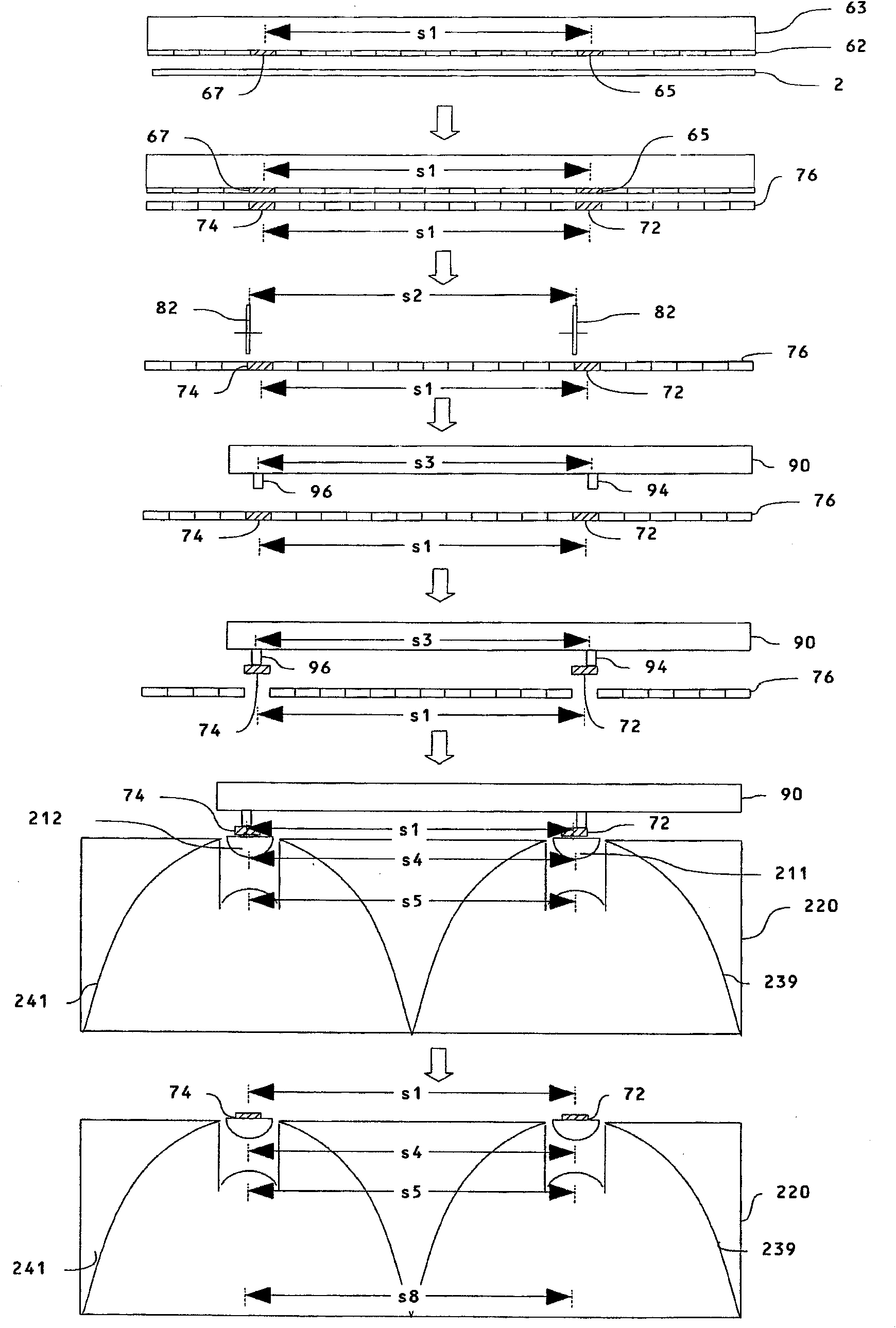
[0161] figure 1 A method of forming a microscopic illumination device is shown in the first example in . In a first step, the monolithic light-emitting element wafer 2 is irradiated using at least one mask 62 mounted on a substrate 63 . For the purposes of this specification, the term monolithic means consisting of one solid or complete component.

[0162] In a second processing step, an array 76 of light-emitting elements is formed on the monolithic wafer 2 . Each element has a position and orientation defined by mask 62 . The mask includes an array of regions, each region defining the structure of at least one layer of the LED chip. Regions 65 and 67 represent the first LED chip and the second LED chip and have a separation s1 as shown. During exposure to wafer 2 through the mask, elements 72 and 74 are formed from regions 65 and 67 of the mask. The spacing s1 of the elements 72, 74 is substantially the same as the spacing of the mask regions 65, 67, and the orientation...


PUM


Abstract

An illumination apparatus and method of manufacture of the same in which an array of light-emitting elements is aligned to an array of optical elements to achieve a thin and efficient light source that can also be arranged to provide directional and/or programmable illumination.

Description

technical field [0001] The invention relates to a lighting device comprising a plurality of light emitting elements aligned with a plurality of optical elements; and also to a method for manufacturing the lighting device. Such devices can be used for domestic or professional lighting, LCD backlighting, and general lighting purposes. Background technique [0002] Incandescent light sources produce a near-black body spectrum, are inexpensive and highly reliable. However, such light sources have very low efficiency and are relatively large, requiring larger lamps. High intensity discharge lamps are capable of producing high luminous flux from a small arc source and are suitable for projection applications and directional lighting, but are bulky. The gas discharge in fluorescent lamps produces pumping of the fluorescent material to produce ultraviolet wavelengths in the visible range. Fluorescent lamps are more efficient than incandescent light sources, but similarly suffer fr...

Claims


Application Information

Patent Timeline
Patent Type & Authority Applications(China)
IPC IPC(8): F21K99/00G02B17/08F21Y101/02H05B44/00
CPCH01L24/83F21Y2105/001F21Y2111/005G02B19/0028F21K9/135H01L2924/01025H01L33/60H01L2224/83801H01L24/78H01L2224/75H01L2224/49107H01L2224/48091F21V5/008F21Y2101/02G02B19/0066F21V5/007H01L2224/85G02B17/0872G02B19/0071H01L2924/01021H01L24/95H01L2924/01079H01L2224/85186H01L24/85H01L2924/01057H01L2924/10253H01L33/58H01L24/75H01L2224/78H01L2924/12041H01L2924/15788H01L2924/00014H01L2924/12042H01L2224/78301H01L2924/181F21Y2105/12F21Y2105/10F21K9/232F21Y2115/10F21Y2107/30H01L24/48H01L24/49H01L2224/75745H01L2224/7598H01L2224/7898H01L2924/3512H01L2924/00H01L2224/45099H01L2224/05599H01L2924/00012H01L2224/4554H01L25/0753H01L27/156
Inventor G·J·伍德盖特J·哈罗德
Owner OPTOVATE
Why Eureka
Try Eureka