
Photodetector with digital three-dimensional package assembly

A technology of structural design and photodetector, which is applied in the direction of electric solid-state devices, semiconductor devices, semiconductor/solid-state device components, etc., can solve the problems of increased difficulty and inconvenience in circuit processing, improve reliability and operability, reduce Difficulty, light weight effect

Active Publication Date: 2012-11-21
BEIJING MXTRONICS CORP +1
View PDF3 Cites 0 Cited by
  • Summary
  • Abstract
  • Description
  • Claims
  • Application Information

AI Technical Summary

Problems solved by technology

[0003] Three-dimensional placement technology is widely used in various fields, including the field of detectors, but the detectors are mostly analog devices, which only simply amplify the signal, and the output needs to be controlled and digitally processed. It increases the difficulty of subsequent circuit processing, especially in systems with strict area requirements, which brings great inconvenience

Method used


Image

  • Photodetector with digital three-dimensional package assembly
  • Photodetector with digital three-dimensional package assembly
  • Photodetector with digital three-dimensional package assembly

Examples


Embodiment Construction

[0028] Below in conjunction with accompanying drawing and specific embodiment the present invention is described in further detail:

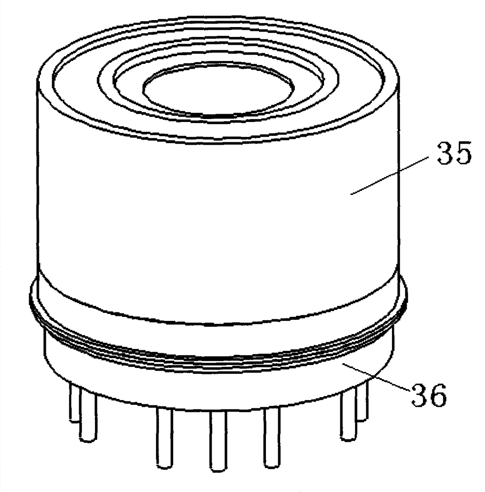
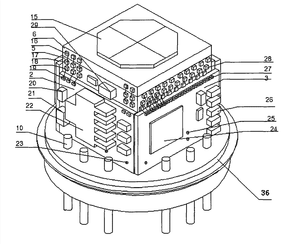
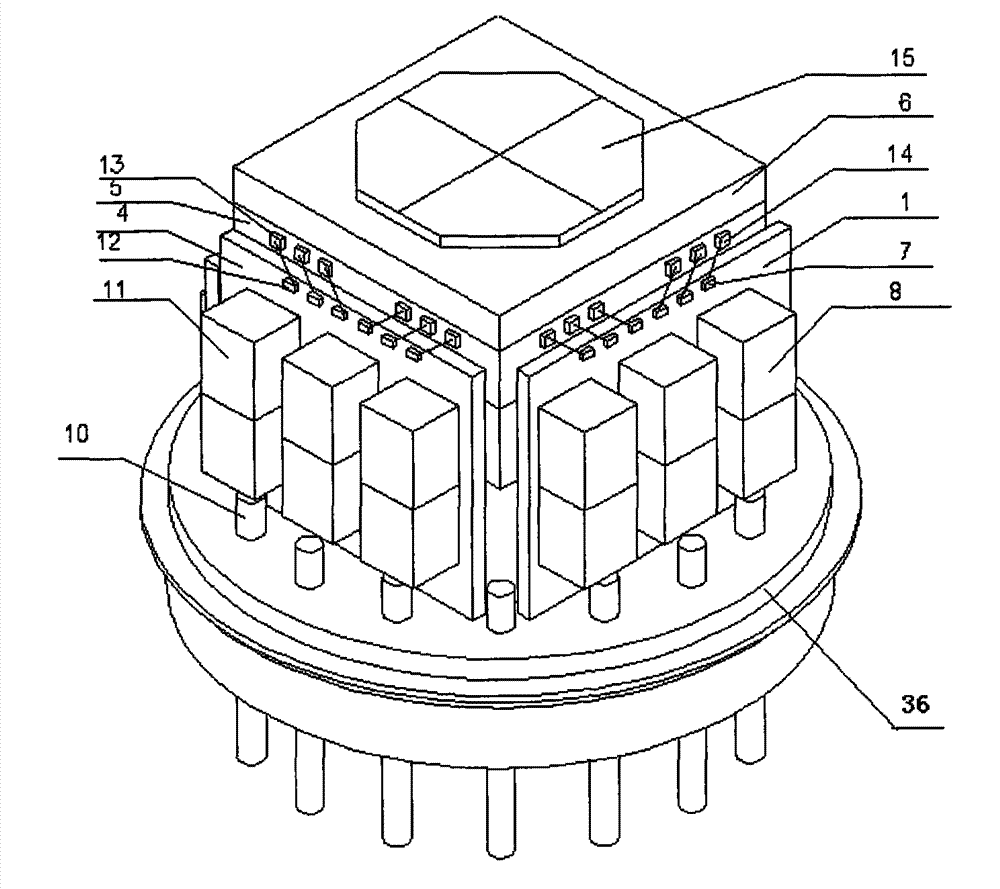
[0029] Such as figure 1 Shown is a schematic diagram of the shell structure in the photodetector of the present invention; Figure 2A It is a schematic diagram of the assembly of the ceramic substrate assembly and the base in the photodetector of the present invention Figure 1 ; Figure 2B It is the second schematic diagram of the assembly of the ceramic substrate assembly and the base in the photodetector of the present invention. The photodetector of the present invention includes a tube case 35, a base 36, a ceramic substrate assembly arranged on the base 36 and placed inside the tube case 35, and a mount Chips and peripheral devices on the ceramic substrate assembly, wherein the shell 35 is a TO25-13 package shell, the ceramic substrate assembly is formed by assembling six ceramic substrates, the first ceramic substrate 1, the second cera...


PUM


Abstract

The invention relates to a photodetector with a digital three-dimensional package assembly. An interconnection structure of six ceramic substrates of the photodetector is characterized in that a method that three-dimensional cabling of the ceramic substrates is combined with a traditional plane bonding technology is adopted, thus the six ceramic substrates, multiple chips and peripheral circuits are assembled in a TO25-13 encapsulation shell; the six ceramic substrates are arranged reasonably so as to stick the chips and the peripheral circuits to the six ceramic substrates; a fifth ceramic substrate is taken as a bridge connection transition substrate; a first to fourth ceramic substrates at four side walls and a sixth ceramic substrate at the top are connected with the fifth ceramic substrate by adopting a traditional wire bonding mode, and the interconnections among the substrates are realized by combining with the method of three-dimensional cabling of the ceramic substrates, thereby ensuring that any two interconnected ceramic substrates are arranged in the same plane, reducing the difficulty of the wire bonding, improving the reliability and the maneuverability and strengthening the antijamming capability. The photodetector is compact in structure, smaller in volume and lighter in weight.

Description

technical field [0001] The invention belongs to the field of microelectronic packaging, and relates to a photodetector with a digital three-dimensional assembly structure design. Background technique [0002] With the rapid development of the microelectronics industry, the role of component packaging in it is becoming more and more important. At present, the trend of device packaging is stronger, smaller and lighter, which requires packaging technology to be multi-functional and high-end. development in the direction of integration. Multi-chip packaging technology is a highly integrated three-dimensional placement technology that emerged on this basis. [0003] Three-dimensional placement technology is widely used in various fields, including the field of detectors, but the detectors are mostly analog devices, which only simply amplify the signal, and the output needs to be controlled and digitally processed. It increases the difficulty of subsequent circuit processing, es...

Claims


Application Information

Patent Timeline
Patent Type & Authority Patents(China)
IPC IPC(8): H01L23/00H01L23/48H01L25/00
Inventor 王恪良李虎明张奇荣
Owner BEIJING MXTRONICS CORP
Learn More