
Method for quickly preparing diamond-silicon carbide electronic packaging material

An electronic packaging material, diamond technology, applied in the direction of circuits, electrical components, electrical solid devices, etc., can solve the limitations of large-scale production and application of diamond-silicon carbide composite materials, limited performance of second-generation packaging materials, single preparation method, etc. problems, to achieve the effect of low-cost preparation, high mechanical and thermal properties, and simple preparation process

Inactive Publication Date: 2012-10-10
UNIV OF SCI & TECH BEIJING
View PDF6 Cites 1 Cited by
  • Summary
  • Abstract
  • Description
  • Claims
  • Application Information

AI Technical Summary

Problems solved by technology

The second generation of electronic packaging materials has been successful, but now the heat generated by electronic components due to the increase in integration and power is rapidly increasing at a rate of four times every three years, and the performance of the second generation of packaging materials is also very limited, so it must Develop third-generation electronic packaging materials with higher thermal conductivity and better thermal stability
However, due to the high thermal stability and hardness of diamond and silicon carbide, the current preparation method of the composite material is very single, requires high equipment, long process cycle, and high production cost, which greatly limits the diamond-silicon carbide composite material. Large-scale production and application of

Method used


Image

  • Method for quickly preparing diamond-silicon carbide electronic packaging material
  • Method for quickly preparing diamond-silicon carbide electronic packaging material

Examples


Embodiment 1

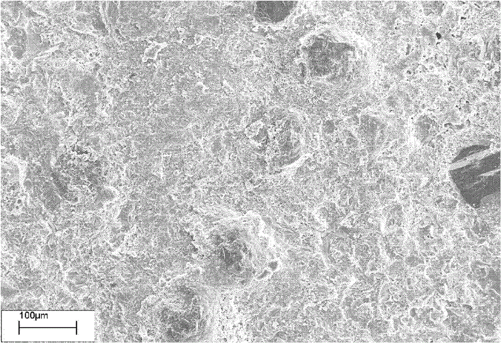
[0016] According to weight percentage, 15% of adhesive phenolic resin, 10% of graphite, 25% of silicon powder with a particle size of -300 mesh, and 50% of diamond particles with a particle size of -100 mesh were wet mixed for 20 hours. Then, the composite blank was obtained by warm pressing at 50MPa pressure and 100°C temperature. Sintered at 1050°C for 24 hours in an argon protective atmosphere, and the density was 3.23g / cm2 after cooling with the furnace. 3 diamond / silicon / carbon porous substrate.

[0017] The prepared diamond / silicon / carbon porous matrix was placed in a graphite crucible, filled with liquid-phase infiltrated pure silicon, and then placed in a high-vacuum sintering furnace for vacuum liquid-phase infiltration for 0.5h, and the infiltration temperature was 1500°C , Vacuum degree -0.01MPa. After cooling with the furnace, a diamond-silicon carbide electronic packaging material with a density of 99.8% can be obtained.

Embodiment 2

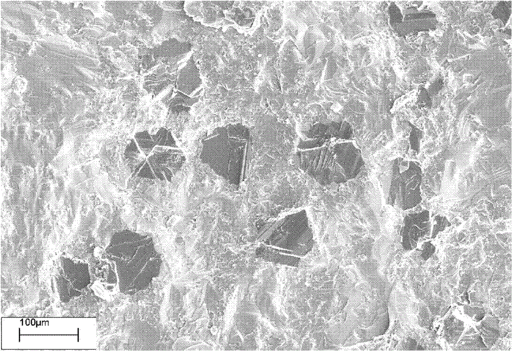
[0019] According to weight percentage, 15% of adhesive phenolic resin, 5% of graphite, 20% of silicon powder with a particle size of -300 mesh, and 60% of diamond particles with a particle size of -500 mesh were wet mixed for 16 hours. Then, the composite blank was obtained by warm pressing under 10MPa pressure and 150°C temperature. Sintered at 1000°C for 24 hours in an argon protective atmosphere, and the density was 3.56g / cm2 after cooling with the furnace. 3 diamond / silicon / carbon porous substrate.

[0020] The prepared diamond / silicon / carbon porous matrix was placed in a graphite crucible, filled with liquid-phase infiltrated pure silicon, and then the whole was placed in a high-vacuum sintering furnace for vacuum liquid-phase infiltration for 1 hour, and the infiltration temperature was 1450°C. Vacuum degree -0.01MPa. After cooling with the furnace, a diamond-silicon carbide electronic packaging material with a density of 99.9% can be obtained.

Embodiment 3

[0022] According to weight percentage, 10% of adhesive phenolic resin, 10% of graphite, 20% of silicon powder with a particle size of -300 mesh, and 60% of diamond particles with a particle size of -500 mesh were wet mixed for 24 hours. Then, the composite blank was obtained by warm pressing under 30MPa pressure and 150°C temperature. Sintered at 1100°C for 24 hours in an argon protective atmosphere, and the density was 3.46g / cm2 after cooling with the furnace. 3 diamond / silicon / carbon porous substrate.

[0023] The prepared diamond / silicon / carbon porous matrix was placed in a graphite crucible, filled with liquid-phase infiltrated pure silicon, and then the whole was placed in a high-vacuum sintering furnace for vacuum liquid-phase infiltration for 0.5h, and the infiltration temperature was 1550°C , Vacuum degree -0.08MPa. After cooling with the furnace, a diamond-silicon carbide electronic packaging material with a density of 99.3% can be obtained.


PUM

PropertyMeasurementUnit
particle size (mesh)aaaaaaaaaa

Abstract

The invention provides a method for preparing a diamond-silicon carbide electronic packaging material fast. The method is characterized in that according to weight percentage, 10-15 percent of adhesive, 5-20 percent of graphite, 20-40 percent of ganister sand and 30-60 percent of diamond are wet-mixed for 16-24h, then a composite material blank is obtained through forming under 100 to 200 DEG C and 10-50MPa pressure; the composite material blank is fired for 16-24h under 1,000 to 1,100 DEG C in the argon atmosphere, and a diamond / silicon / carbon polyporous matrix having a certain strength andporosity is obtained after cooling; the diamond / silicon / carbon polyporous matrix prepared is placed in a graphite crucible and then is embedded through liquidphase infiltration infiltrated material,and then the crucible is placed in a high vacuum fritting furnace for vacuum liquidphase infiltration for 0.5-1h, and the infiltration temperature is 1,450-1,550 DEG C, and the vacuum degree is -0.08to -0.01MPa; and the compact diamond-silicon carbide electronic packaging material can be obtained after cooling.

Description

technical field [0001] The invention belongs to a method for rapidly preparing an electronic packaging material, in particular to a preparation method of a diamond-silicon carbide electronic packaging material. Background technique [0002] Electronic components play an extremely important role in industrial development, and their application fields are becoming more and more extensive. In order to meet the new requirements of various fields due to continuous development, the performance of electronic components is also constantly improving. Facts have proved that only electronic components with greater power, smaller size, lighter weight, higher integration density, higher performance, and lower cost can meet the needs of future industrial development. However, the higher the power and the smaller the size of electronic components, their stability and life will be greatly affected by the high calorific value, which also puts forward higher requirements for the thermal condu...

Claims


Application Information

Patent Timeline
Patent Type & Authority Patents(China)
IPC IPC(8): H01L21/56H01L23/29
Inventor 何新波杨振亮吴茂刘荣军任淑彬曲选辉
Owner UNIV OF SCI & TECH BEIJING
Learn More