

High-power base plate effectively integrating circuit board and radiator and manufacturing method thereof
A manufacturing method and circuit board technology, applied in the direction of circuits, electric solid-state devices, semiconductor devices, etc., can solve the problems affecting the quality and life stability of high-power LED street lamps, the heat of LED lamps cannot be exported in time, and thermal obstacles, etc., to achieve The effect of low price, easy purchase and stable performance
- Summary
- Abstract
- Description
- Claims
- Application Information
AI Technical Summary
Problems solved by technology
Method used
Image

Examples
Embodiment 1
[0041] Taking high-power LED lighting equipment as an example, the specific structure and manufacturing method of the present invention are described in comparison.
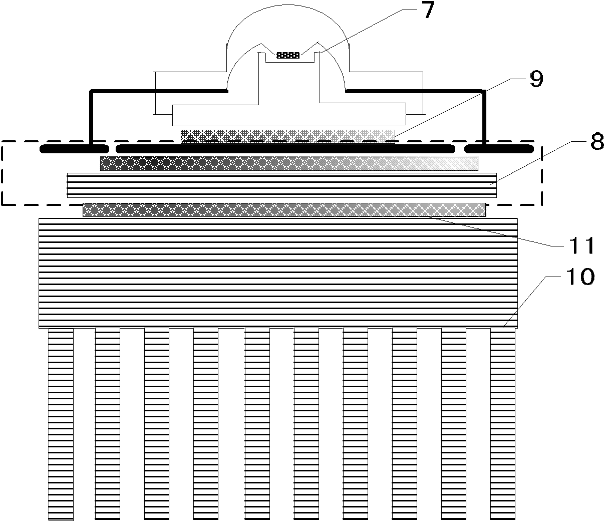
[0042] Such as figure 1As shown, the heat dissipation mode of the traditional LED lamp is: the electronic component 7 (LED lamp) is connected to the aluminum substrate 8, the thermal conductive silica gel 9 is coated between the electronic component 7 and the aluminum substrate 8, and the aluminum substrate 8 includes soldering copper foil, epoxy resin Or insulating material and aluminum alloy sheet. An aluminum alloy heat sink 10 is installed under the aluminum base plate 8 , and thermal conductive silicon grease 11 is coated between the aluminum base plate 8 and the aluminum alloy heat sink 10 .
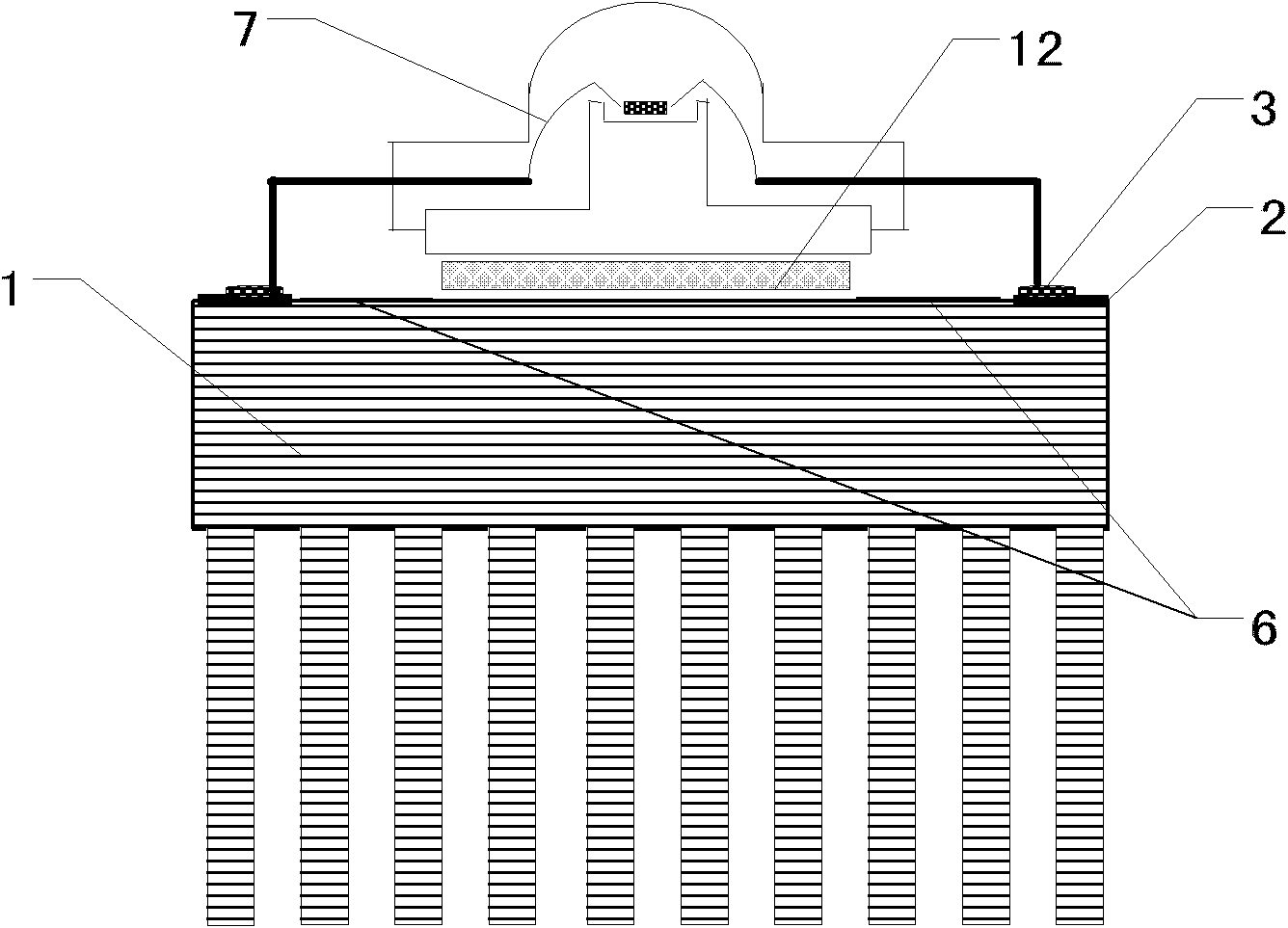
[0043] Such as figure 2 As shown, the heat dissipation method of the present invention is: the electronic component 7 is directly bonded or welded on the metal heat dissipation plate 1, which avoids the heat dissip...
Embodiment 2
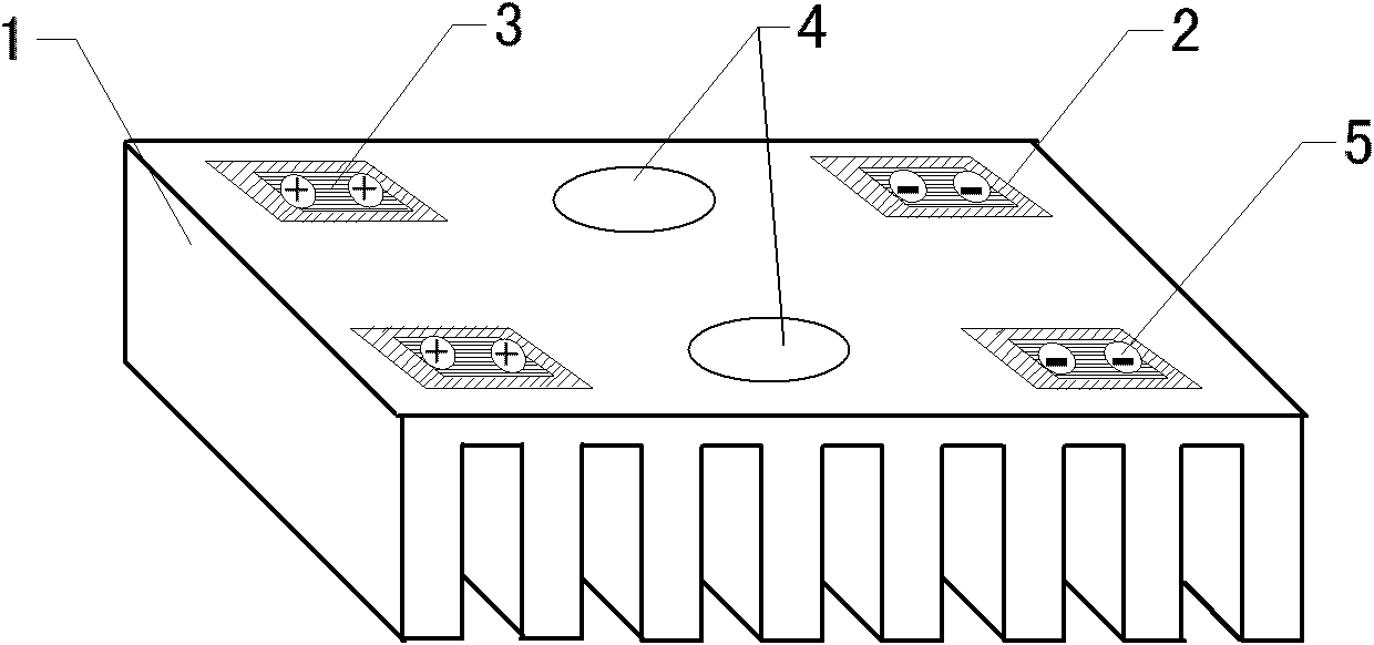
[0058] The electronic component installation area 4 is fixed with an electronic component 7 through the insulating ceramic glue 12, and the circuit area is covered with a heat-conducting and insulating ceramic circuit layer 2 formed by the insulating ceramic glue 12, and the thickness of the heat-conducting and insulating ceramic circuit layer 2 is between 0.1 and 0.3 mm , thermally conductive and insulating ceramic circuit layer 2 is covered with copper foil circuit 3, solder joint 5 is arranged on copper foil circuit 3, and waterproof insulation is sprayed on the surface of metal heat sink 1 except solder joint 5 and electronic component installation area 4 paint6.
[0059] The steps of the manufacturing method of the high-power substrate in which the circuit board and the heat sink are efficiently integrated are as follows:
[0060] a. The area on the metal cooling plate 1 except the electronic component installation area 4 is coated with insulating ceramic glue 12, and a l...
Embodiment 3
[0068] The manufacturing method of the high-power substrate in which the circuit board and the radiator are efficiently integrated can also be:
[0069] a. Print the insulating ceramic glue 12 on the area of the metal heat dissipation plate 1 except the electronic component installation area 4 through screen printing, and make the heat-conducting and insulating ceramic circuit layer 2, and the thickness of the heat-conducting and insulating ceramic circuit layer 2 is between 0.1 and 0.3 mm. ;
[0070] b. After the insulating ceramic circuit layer 2 is cured at 120-180°C for 5-15 minutes, a layer of solderable conductive copper paste is printed on the heat-conducting insulating ceramic circuit layer 2 through a screen to form a copper foil circuit 3;
[0071] c. For the copper foil circuit 3 formed by screen printing solderable conductive copper paste, directly cure at 120-180°C for 10-25 minutes;
[0072] d. Perform tin spraying treatment on each solder joint 5 on the coppe...
PUM
| Property | Measurement | Unit |
|---|---|---|
| Thickness | aaaaa | aaaaa |
| Thickness | aaaaa | aaaaa |
| Thermal conductivity | aaaaa | aaaaa |
Abstract
Description
Claims
Application Information