Nitride light-emitting diode (LED) structure and preparation method thereof
An LED structure, nitride technology, applied in electrical components, circuits, semiconductor devices, etc., can solve the problems of low hole tunneling probability, low carrier confinement, and inability to improve the uniformity of carrier distribution, etc. Achieve the effect of improving uniformity, improving internal quantum efficiency and luminous intensity, and improving recombination efficiency
- Summary
- Abstract
- Description
- Claims
- Application Information
AI Technical Summary
Problems solved by technology
Method used
Image

Examples
Embodiment Construction
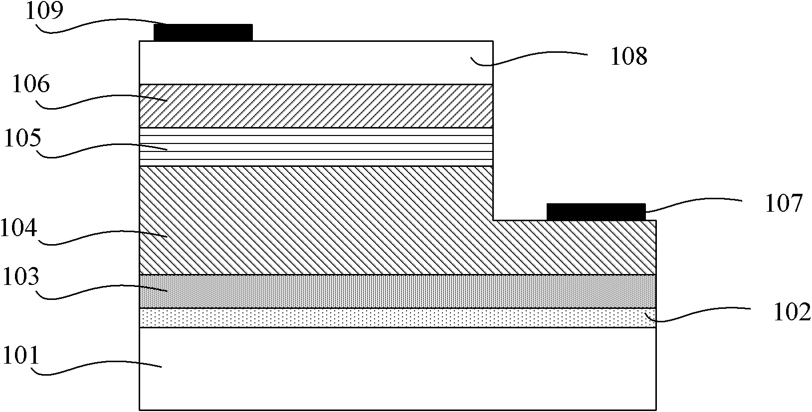
[0032] The structure and preparation method of the nitride LED proposed by the present invention will be further described in detail below with reference to the accompanying drawings and specific examples. Advantages and features of the present invention will be apparent from the following description and claims. It should be noted that all the drawings are in very simplified form and use imprecise ratios, which are only used for the purpose of conveniently and clearly assisting in describing the embodiments of the present invention.
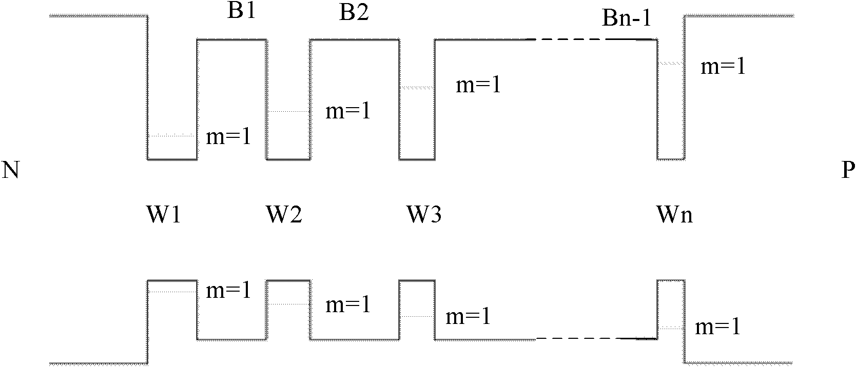
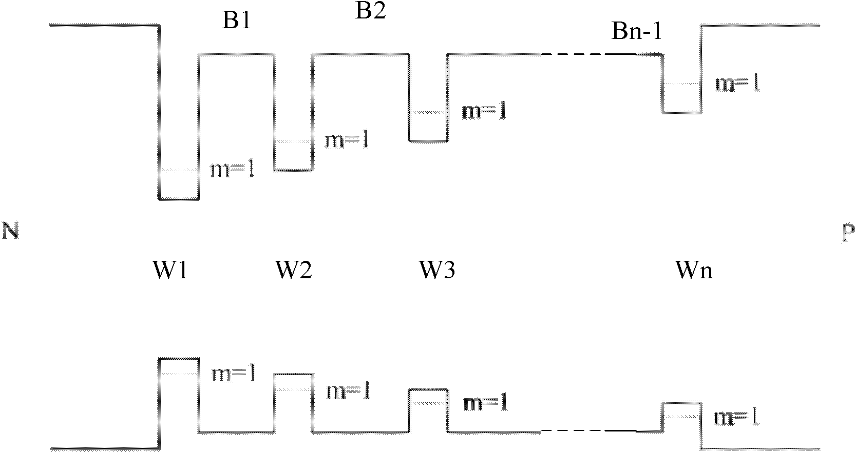
[0033]The core idea of the present invention is to provide a nitride LED structure. Under the premise that the transition energy between the ground state energy levels of the quantum wells in the multi-quantum well active layer gradually changes, the LED structure gradually changes the potential of the quantum wells. The width of the barrier can improve the uniformity of carrier distribution in the active region. While considering the quantum ...
PUM
 Abstract
Description
Claims
Application Information
 - Generate Ideas
- Intellectual Property
- Life Sciences
- Materials
- Tech Scout
- Unparalleled Data Quality
- Higher Quality Content
- 60% Fewer Hallucinations
Browse by: Latest US Patents, China's latest patents, Technical Efficacy Thesaurus, Application Domain, Technology Topic, Popular Technical Reports.
© 2025 PatSnap. All rights reserved.Legal|Privacy policy|Modern Slavery Act Transparency Statement|Sitemap|About US| Contact US: help@patsnap.com