
Semiconductor device, method for producing the semiconductor device, substrate for semiconductor element and method for producing the substrate

A technology for semiconductors and components, applied in the field of substrates for semiconductor components, can solve the problems of semiconductor production and processing temperature limit, difficulty in forming strong bonds, and decrease in contact area, and achieve the effects of improving electron mobility, improving performance, and suppressing separation.

Inactive Publication Date: 2011-09-21
FUJIFILM CORP
View PDF13 Cites 6 Cited by
  • Summary
  • Abstract
  • Description
  • Claims
  • Application Information

AI Technical Summary

Problems solved by technology

However, these substrates have lower heat resistance compared with conventional glass substrates, so there is a problem that semiconductor production processing temperatures are limited to temperatures close to room temperature
[0011] There is a problem that when nanoporous silica is formed as a film on a substrate, cracks appear every few millimeters
However, in the case where a porous layer is formed on a substrate, since the actual contact area decreases, especially as the porosity increases, it becomes difficult to form a strong bond between the two.

Method used


Image

  • Semiconductor device, method for producing the semiconductor device, substrate for semiconductor element and method for producing the substrate
  • Semiconductor device, method for producing the semiconductor device, substrate for semiconductor element and method for producing the substrate
  • Semiconductor device, method for producing the semiconductor device, substrate for semiconductor element and method for producing the substrate

Examples


Embodiment approach 1

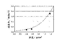
[0100] 15 parts of 10 mM acetic acid solution, 2 parts of Pluronic F-127 (block copolymer surfactant from BASF), 1 part of urea and 9 parts of methyltrimethoxysilane were mixed to obtain a clear solution. Place the solution in a semi-hermetically sealed Teflon TM In the container, a gelation reaction was performed at 80° C. for 2 days. Surfactants were removed from the wet gel by washing in boiling water, and solvent exchange was performed with methanol and fluorosolvent (Novec-7100 from Sumitomo 3M). The gel was dried to obtain a transparent xerogel porous structure formed of polymethylsilsesquioxane. The density ρ of the xerogel measured by the Archimedes method is 0.40 g / cm 3 .

Embodiment approach 2

[0102] A translucent xerogel formed of polymethylsilsesquioxane was obtained by the same procedure as Embodiment 1 (except that the amount of Pluronic F-127 was changed to 1.5 parts). The density ρ of the dry gel measured by the Archimedes method is 0.57g / cm 3 .

Embodiment approach 3

[0104] By the same procedure as Embodiment 1 (the difference is that by mixing 35 parts of 10 mM acetic acid solution, 16 parts of tetramethoxysilane, 10 parts of methyltrimethoxysilane, 5.5 parts of Pluronic F-127 and 2.5 parts Parts of urea to obtain a transparent solution) to obtain a transparent xerogel formed from a copolymer of methylsilsesquioxane and siloxane. The weight ratio of siloxane skeleton / silsesquioxane skeleton calculated from the mixing ratio was 61 / 39. The density ρ of the xerogel measured by the Archimedes method is 0.40 g / cm 3 .


PUM

PropertyMeasurementUnit
densityaaaaaaaaaa
diameteraaaaaaaaaa
thermal degradation temperatureaaaaaaaaaa

Abstract

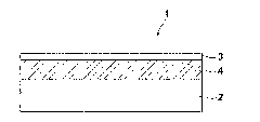
A semiconductor device is provided with a porous structure layer (4) formed by silicone resin between a substrate (2) and a semiconductor element (3). Alternatively, a porous layer (24) having a density of 0.7g / cm 3 or less, formed by a compound obtained by hydrolyzing and condensing at least one type of alkoxysilane selected from a group consisting of monoalkoxysilane, dialkoxysilane, and trialkoxysilane, and tetraalkoxysilane is provided between a substrate (22) and a semiconductor element (23) of a semiconductor device (21). As a further alternative, an adhesion layer (33) formed by a compound obtained by hydrolyzing and condensing an alkoxysilane is provided on a resin substrate (32), and a porous layer (34) having a density of 0.7g / cm 3 or less, formed by a compound obtained by hydrolyzing and condensing an alkoxysilane, is provided on the adhesion layer (33).

Description

technical field [0001] The present invention relates to semiconductor devices such as solar cells, thin film transistor circuits, and displays (image display devices), and methods of manufacturing semiconductor devices. The present invention also relates to a substrate for a semiconductor element and a method for manufacturing the substrate. Background technique [0002] In order to form flexible semiconductor devices, such as displays and thin-film solar cells, a lot of research has been done. In order to make these devices flexible, resin films such as PET and polyimide are used as substrates. However, these substrates have lower heat resistance compared with conventional glass substrates, so there is a problem that semiconductor production processing temperatures are limited to temperatures close to room temperature. Furthermore, semiconductors produced by high temperature processes often exhibit favorable semiconducting properties. This is an obstacle to obtaining a s...

Claims


Application Information

Patent Timeline
Patent Type & Authority Applications(China)
IPC IPC(8): H01L23/14H01L21/02H01L21/48C08L83/04
CPCH01L27/1266H01L27/1214H01L27/1218H01L21/324H01L21/02381H01L29/78603H01L27/1262
Inventor 佐藤圭吾祐谷重德
Owner FUJIFILM CORP
Learn More