Semiconductor device

A technology of semiconductors and devices, which is applied in the field of passive semiconductor devices, can solve problems affecting process window control, etc., and achieve the effects of ensuring process stability, good patterning density, and good quality factor

Active Publication Date: 2011-09-21
SEMICON MFG INT (SHANGHAI) CORP +1
View PDF5 Cites 7 Cited by
  • Summary
  • Abstract
  • Description
  • Claims
  • Application Information

AI Technical Summary

Problems solved by technology

But this requirement affects the control of the entire process window

Method used


Image

  • Semiconductor device
  • Semiconductor device
  • Semiconductor device

Examples


Embodiment Construction

[0020] In the following description, numerous specific details are given in order to provide a more thorough understanding of the present invention. It will be apparent, however, to one skilled in the art that the present invention may be practiced without one or more of these details. In other examples, some technical features known in the art are not described in order to avoid confusion with the present invention.

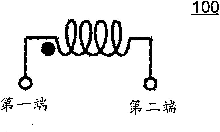
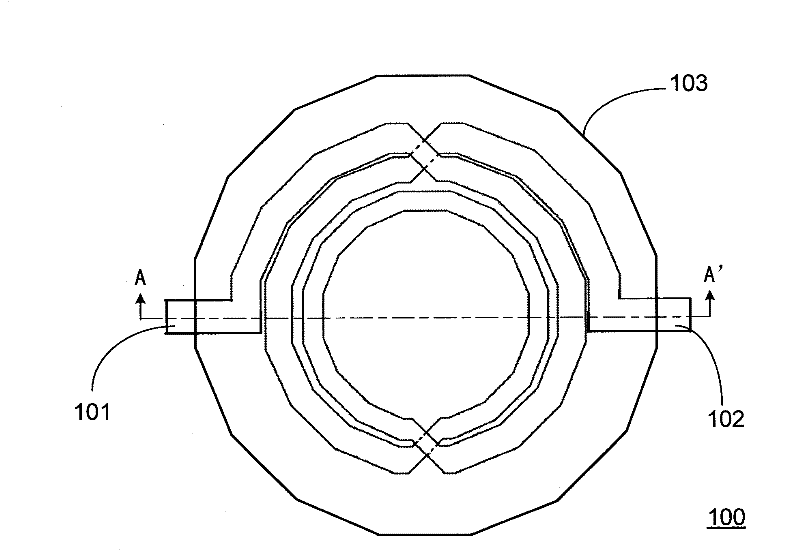
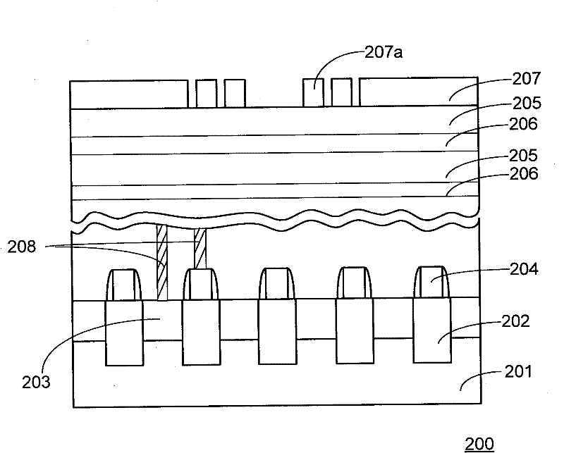
[0021] In order to thoroughly understand the present invention, detailed steps will be presented in the following description to illustrate how the present invention provides a planar inductor based on CMOS technology to solve the above problems. Obviously, the practice of the invention is not limited to specific details familiar to those skilled in the semiconductor arts. Preferred embodiments of the present invention are described in detail below, however, the present invention may have other embodiments besides these detailed descriptions.

[0022] Accordin...


PUM


Abstract

The invention provides a semiconductor device, which comprises a substrate, a plurality of shallow isolation grooves, a plurality of active regions, a polycrystalline silicon layer, a plurality of interlayer dielectric layers, a first metal layer, a second metal layer and a patterned grounding shielding layer, wherein the plurality of shallow isolation grooves are formed in the substrate; the plurality of active regions are formed in the substrate; adjacent active regions are spaced through the plurality of shallow isolation grooves; the polycrystalline silicon layer is formed on the plurality of shallow isolation grooves; the plurality of interlayer dielectric layers are formed in the active regions and on the polycrystalline silicon layer; the first metal layer is sandwiched between adjacent interlayer dielectric layers; the second metal layer is formed on the interlayer dielectric layers which are positioned on a top layer and is used for forming planar induction; and the patterned grounding shielding layer is formed by grounding the active regions and the polycrystalline silicon layer through contact holes which are formed in the interlayer dielectric layers. According to the device, compared with planar induction without the patterned grounding shielding layer, the planar induction inserted into the patterned grounding shielding layer provides comparability or better Q performance, and the influence of induced substrate coupled noise on a circuit can be reduced.

Description

technical field [0001] The invention relates to a passive semiconductor device, in particular to a planar inductor in a radio frequency integrated circuit based on complementary metal oxide semiconductor (CMOS) technology. Background technique [0002] The huge demand of the rapidly growing wireless communication market has also created the demand for radio frequency integrated circuits. In recent years, with the continuous reduction of feature size, the characteristic frequency of MOSFET in deep submicron CMOS process has reached above 50 GHz, making it possible to realize high-frequency analog circuits in the GHz band using CMOS process. In recent years, researchers from all over the world have done a lot of research on the design and production of CMOS radio frequency integrated circuits, which has continuously improved the performance of CMOS radio frequency integrated circuits. [0003] Planar inductors (or on-chip inductors) are key components in RF integrated circuit...

Claims


Application Information

Patent Timeline
Patent Type & Authority Applications(China)
IPC IPC(8): H01L27/04
Inventor 程仁豪
Owner SEMICON MFG INT (SHANGHAI) CORP
Why Eureka
Try Eureka