P-type ZnO and n-type GaN combined ZnO-based light-emitting devices and manufacturing methods thereof

A light-emitting device, p-type technology, applied in the direction of semiconductor devices, electrical components, circuits, etc., can solve the problem of short light-emitting wavelength, achieve the effect of overcoming the narrow band gap and expanding the application range

Inactive Publication Date: 2011-09-21
EPITOP PHOTOELECTRIC TECH
View PDF11 Cites 1 Cited by
  • Summary
  • Abstract
  • Description
  • Claims
  • Application Information

AI Technical Summary

Problems solved by technology

In addition, the band gap of n-type GaN is slightly wider than that of ZnO, so it is possible to confine carriers without prep...

Method used


Image

  • P-type ZnO and n-type GaN combined ZnO-based light-emitting devices and manufacturing methods thereof
  • P-type ZnO and n-type GaN combined ZnO-based light-emitting devices and manufacturing methods thereof
  • P-type ZnO and n-type GaN combined ZnO-based light-emitting devices and manufacturing methods thereof

Examples


Embodiment 1

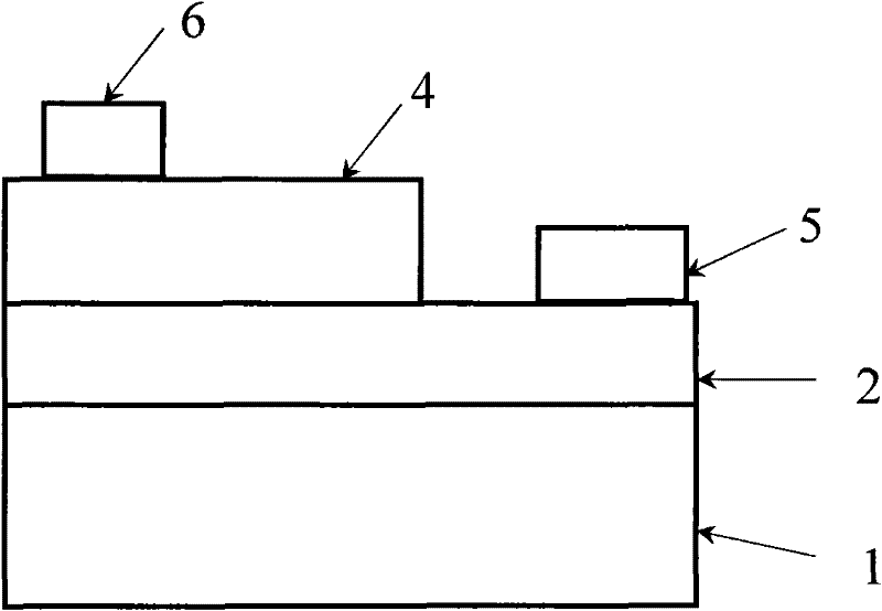
[0024] ZnO-based light-emitting devices combining p-type ZnO and n-type GaN without a current lower confinement layer. The structure of this ZnO-based light-emitting device combined with p-type ZnO and n-type GaN without a current lower confinement layer is shown in the appendix figure 2 , characterized in that the GaN epitaxial layer 2 is an n-type GaN thin film material, no current lower confinement layer 3 is prepared, the ZnO light-emitting layer 4 is a p-type ZnO-based thin film material, and a p-type ZnO-based material is directly prepared on the n-type GaN epitaxial layer 2 to emit light Layer 4.

[0025] Its preparation process is, with Al 2 o 3 substrate as an example, using the current mature conventional MOCVD process on Al 2 o 3 The substrate grows an n-type (such as Si-doped) GaN epitaxial layer 2 of 1 to 10 microns, and the carrier concentration is 10 18 ~10 20 / cm 3 , and then adopt the MOCVD method, especially the special ZnO film growth MOCVD equipment...

Embodiment 2

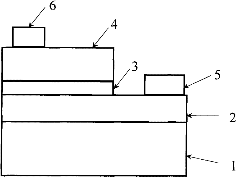
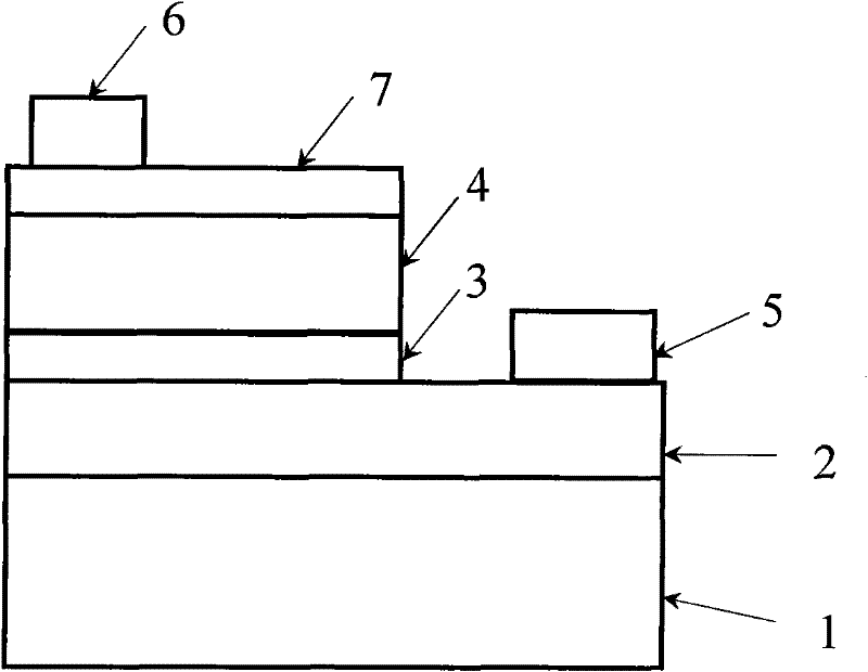
[0027] A ZnO-based light-emitting device based on the combination of p-type ZnO and n-type GaN under the current confinement layer of AlGaN thin film material. The ZnO-based light-emitting device structure of the combination of p-type ZnO and n-type GaN under the current confinement layer of this AlGaN thin film material is shown in the appendix figure 1 , the structure and preparation process of the GaN epitaxial layer 2 and the ZnO light-emitting layer 4 are the same as in Example 1, which is characterized in that a layer of current limiting layer 3 is grown on the GaN epitaxial layer 2, and the current limiting layer 3 of this layer is n Type Alx Ga 1-x N material thin film, wherein the value of x is in the range of 0.01 to 0.5; the preparation process is as follows: Al 2 o 3 substrate as an example, using the current mature conventional MOCVD process method on Al 2 o 3 The substrate grows an n-type GaN epitaxial layer 2 including a buffer layer of 1 to 10 microns, and ...

Embodiment 3

[0029] Ga 2 o 3 ZnO-based light-emitting devices combining p-type ZnO and n-type GaN under the current confinement layer of thin film materials. This Ga 2 o 3 See the attached figure 1 , the structure and preparation process of the GaN epitaxial layer 2 and the ZnO light-emitting layer 4 are the same as in Example 1, and it is characterized in that a layer of Ga is prepared on the GaN epitaxial layer 2 2 o 3 Material thin film current lower confinement layer 3; its preparation process except Ga 2 o 3 Except for the different manufacturing process of the current lower confinement layer 3 of the material thin film, the rest of the process is the same as that of Embodiment 2; devices with this structure can also use n-type SiC single crystal substrates.

[0030] Ga 2 o 3 There are two methods for preparing the material thin film current confinement layer 3:

[0031] One is prepared by MOCVD method. The Ga source can be trimethylgallium (TMGa) or triethylgallium (TEGa). ...


PUM

PropertyMeasurementUnit
Thicknessaaaaaaaaaa
Thicknessaaaaaaaaaa

Abstract

The invention belongs to the technical fields of semiconductor light-emitting devices and manufacturing methods thereof and in particular relates to a plurality of kinds of p-type ZnO and n-type GaN combined ZnO-based light-emitting devices and manufacturing methods thereof. One device comprises a substrate, a GaN epitaxial layer, a current lower limiting layer, a lower electrode, a ZnO-based light-emitting layer and an upper electrode, wherein the GaN epitaxial layer epitaxially grows on the substrate; the current lower limiting layer and the lower electrode are manufactured on the epitaxiallayer in a mutually discrete way; the ZnO-based light-emitting layer is manufactured on the current lower limiting layer; and the upper electrode is manufactured on the ZnO-based light-emitting layer; and more particularly, the GaN epitaxial layer is an n-type GaN film, the current lower limiting layer is an n-type AlGaN/Ga2O3 film, and the ZnO-based light-emitting layer is a p-type ZnO-based film. The invention also relates to a ZnO-based light-emitting device with the current lower limiting layer and a ZnO-based light-emitting device with a current upper limiting layer. By means of the p-type ZnO and n-type GaN combined ZnO-based light-emitting devices and the manufacturing methods thereof disclosed by the invention, the defects, such as lower concentration of a p-type GaN epitaxial carrier, large series resistance of the device, high working voltage of the device, and low output power of the device are overcome, and the application range of the devices is further broadened.

Description

technical field [0001] The invention belongs to the technical field of semiconductor light-emitting devices and their preparation, and in particular relates to the structure of a light-emitting device based on ZnO-based materials and its manufacturing method. Background technique [0002] GaN-based materials have wider application prospects in the field of solid-state lighting. The energy band gap and lattice constant of ZnO and GaN are very close, and they have similar photoelectric properties. However, compared with GaN, ZnO has a higher melting point and exciton binding energy, higher exciton gain, lower epitaxial growth temperature, lower cost, and easy etching, which makes the subsequent processing of the epitaxial wafer easier and makes the device The preparation is more convenient and so on. Therefore, the successful development of ZnO-based light-emitting tubes and lasers may replace or partially replace GaN-based optoelectronic devices, and will have greater appli...

Claims


Application Information

Patent Timeline
IPC IPC(8): H01L33/14H01L33/26
Inventor 杜国同夏晓川赵旺梁红伟张宝林
Owner EPITOP PHOTOELECTRIC TECH
Why Eureka
Try Eureka