

GaN-based multi-quantum well super light-emitting diode (SLED) and preparation method thereof
A technology of superluminescence and multiple quantum wells, which is applied in the field of third-generation semiconductor material GaN-based multi-quantum well superluminescent light-emitting diodes and its preparation, can solve the problems of low output power of GaN-based LEDs, and achieve the goal of overcoming difficulties in realization and output High power, simple preparation effect
- Summary
- Abstract
- Description
- Claims
- Application Information
AI Technical Summary
Problems solved by technology
Method used
Image

Examples
Embodiment 1
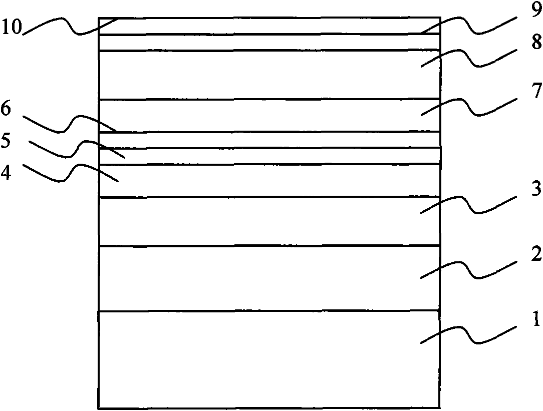
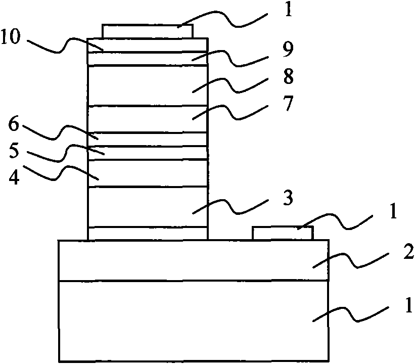
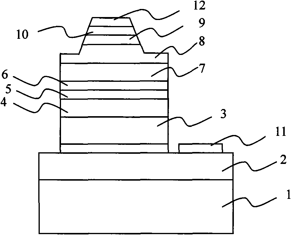
[0054] see figure 1 , the epitaxial wafer preparation method is given below:
[0055] (1) The sapphire substrate 1 of (0001) orientation no-cleaning is packed into reaction chamber, in H 2 Under atmosphere, heat to 1060°C and bake for 10 minutes, and the pressure in the reaction chamber is 500 Torr.
[0056] (2) A low-temperature GaN buffer layer with a thickness of 25nm was grown at 530°C (at figure 1 Not shown in ), the growth pressure is 300Torr, the flow rate of TMGa is 40μmol / min, NH 3 The flow rate is 80mol / min.
[0057] (3) The N-type GaN electrode contact layer 2 is grown at 1030° C., and the growth pressure is 100 Torr.
[0058] (4) 60 pairs of N-type AlGaN / GaN superlattice optical confinement layers 3 were grown at 1050° C., the growth pressure was 50 Torr, and the periodic thickness was 6 nm.
[0059] (5) The N-type GaN waveguide layer 4 is grown at 1030° C., the growth pressure is 200 Torr, and the growth thickness is 0.1 μm.
[0060] (6) Lowering the tempera...
Embodiment 2
[0069] The epitaxial wafer preparation method is given below:
[0070] (1) Load the (0001) orientation no-clean sapphire substrate into the reaction chamber, and 2 Under atmosphere, heat to 1060°C and bake for 10 minutes, and the pressure in the reaction chamber is 400 Torr.
[0071] (2) A low-temperature GaN buffer layer with a thickness of 30nm was grown at 550°C, the growth pressure was 400Torr, the flow rate of TMGa was 50μmol / min, and NH 3 The flow rate is 100mol / min.
[0072] (3) The N-type GaN electrode contact layer is grown at 1050° C. with a growth pressure of 150 Torr.
[0073] (4) 120 pairs of N-type AlGaN / GaN superlattice optical confinement layers were grown at 1080° C. with a growth pressure of 75 Torr and a periodic thickness of 5 nm.
[0074] (5) The N-type GaN waveguide layer is grown at 1050° C., the growth pressure is 100 Torr, and the growth thickness is 0.15 μm.
[0075] (6) Lowering the temperature and growing the InGaN / GaN multi-quantum well active ...
Embodiment 3
[0084] The epitaxial wafer preparation method is given below:
[0085] (1) Load the (0001) orientation no-clean sapphire substrate into the reaction chamber, and 2 Heating to 1060° C. and baking for 10 minutes under atmosphere, and the pressure in the reaction chamber is 300 Torr.
[0086] (2) A low-temperature GaN buffer layer with a thickness of 40nm was grown at 580°C, the growth pressure was 500Torr, the flow rate of TMGa was 60μmol / min, and NH 3 The flow rate is 120mol / min.
[0087] (3) The N-type GaN electrode contact layer is grown at 1030° C., and the growth pressure is 200 Torr.
[0088] (4) 180 pairs of N-type AlGaN / GaN superlattice optical confinement were grown at 1150°C, the growth pressure was 100 Torr, and the period thickness was 4nm.
[0089] (5) The N-type GaN waveguide layer is grown at 1030° C. with a growth pressure of 150 Torr. The growth thickness was 0.1 μm.
[0090] (6) Lowering the temperature and growing the InGaN / GaN multi-quantum well active l...
PUM
| Property | Measurement | Unit |
|---|---|---|
| Thickness | aaaaa | aaaaa |
| Thickness | aaaaa | aaaaa |
| Thickness | aaaaa | aaaaa |
Abstract
Description
Claims
Application Information