Magnetic nanostructures for tco replacement

A magnetic nano, magnetic metal nano technology, applied in the direction of nanostructure manufacturing, oxide conductors, magnetic objects, etc., can solve the problem of low optical transparency, the combination of electrical conductivity and optical transparency has not been fully optimized, and nano silver cannot be used effectively Line and other issues

Inactive Publication Date: 2011-09-21
APPLIED MATERIALS INC
View PDF0 Cites 10 Cited by
  • Summary
  • Abstract
  • Description
  • Claims
  • Application Information

AI Technical Summary

Problems solved by technology

as in figure 2 As seen in , the current path through the thin film 210 is rather convoluted, and the silver nanowires 220 cannot be effectively used
Furthermore, because the silver nanowires 220 are not effectively used to provide electrical conductivity to the film 210, the film 210 has less optimal optical transparency, clearly, the combination of electrical conductivity and optical transparency obtained from films comprising nanowires has not yet been achieved. fully optimized

Method used


Image

  • Magnetic nanostructures for tco replacement
  • Magnetic nanostructures for tco replacement
  • Magnetic nanostructures for tco replacement

Examples


Embodiment Construction

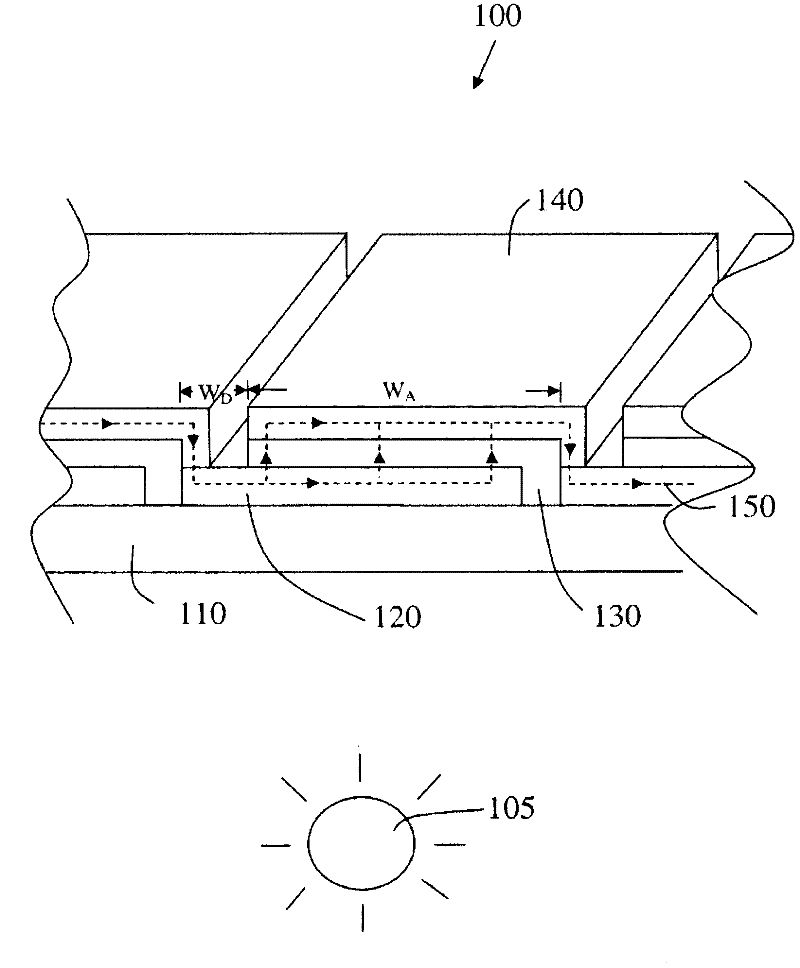
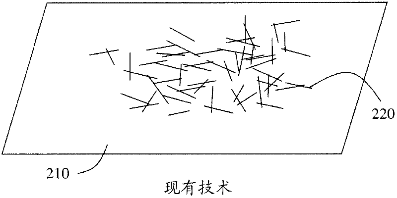
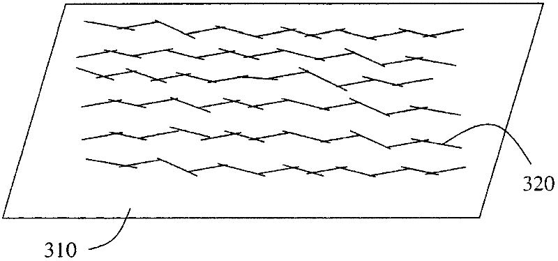
[0022] The present invention will now be described in detail with reference to the accompanying drawings, which are provided as illustrative examples of the invention so as to enable those skilled in the art to operate the invention. It should be noted that the figures and examples described below are not intended to limit the scope of the invention to a single embodiment, but other embodiments are possible by exchanging some or all of the depicted or illustrated components. Moreover, some components of the present invention may be partially or completely implemented using known components, and only some of the known components required for understanding the present invention will be described here, and detailed descriptions of other parts of such known components will be omitted. The description is so as not to obscure the invention. In this specification, an embodiment showing a single component should not be considered limiting; rather, the invention is intended to cover ot...


PUM

PropertyMeasurementUnit
diameteraaaaaaaaaa
diameteraaaaaaaaaa
diameteraaaaaaaaaa

Abstract

This invention provides an optically transparent electrically conductive layer with a desirable combination of low electrical sheet resistance and good optical transparency. The conductive layer comprises a multiplicity of magnetic nanostructures in a plane, aligned into a plurality of roughly parallel continuous conductive pathways, wherein the density of the magnetic nanostructures allows for substantial optical transparency of the conductive layer. The magnetic nanostructures may be nanoparticles, nanowires or compound nanowires. A compound magnetic nanowire may comprise a silver nanowire covered by a layer of magnetic metal such as nickel or cobalt. Furthermore, a compound magnetic nanowire may comprise a carbon nanotube (CNT) attached to a magnetic metal nanowire. A method of forming the conductive layer on a substrate includes: depositing a multiplicity of magnetic nanostructures on the substrate and applying a magnetic field to form the nanostructures into a plurality of conductive pathways parallel to the surface of the substrate.

Description

technical field [0001] The present invention relates generally to transparent conductive films, and more particularly to transparent conductive films comprising magnetic nanostructures such as nanowires and nanoparticles. Background technique [0002] Optically transparent conductive layers can be used in a variety of applications where a transparent conductor is required, or can provide advantages. Applications using transparent conductors include: liquid crystal displays, plasma displays, organic light-emitting diodes, solar cells, and more. Transparent conductive oxides (TCO) such as ITO and ZnO are the most commonly used transparent conductive materials. However, TCO films have a trade-off between conductivity and optical transparency—when the carrier concentration is increased to enhance conductivity, optical transparency decreases, and vice versa. Furthermore, when the thickness of the TCO film is increased to increase the sheet resistance, the optical transparency d...

Claims


Application Information

Patent Timeline
Patent Type & Authority Applications(China)
IPC IPC(8): H01B1/00B82B3/00C08J5/18B82B1/00
CPCH01B1/04H01B1/02H01B1/08H01J2217/49207H01L51/5206B82Y25/00H01J9/02H01F1/0081H01F1/445H01F1/0054Y10T29/49206H01B5/14H01B1/00B82B3/00B82B1/00H10K50/81
Inventor S·文哈弗贝克O·那拉玛苏N·M·克里希纳V·L·普施帕拉吉R·古克
Owner APPLIED MATERIALS INC
Why Eureka
Try Eureka