Large aluminum nitride crystals with reduced defects and methods of making them

a technology of aluminum nitride crystals and defects, which is applied in the field of large aluminum nitride crystals with reduced defects and methods of making them, can solve the problems of reducing reducing the optical transparency, and reducing the number of problems, so as to facilitate the practical crystal production strategy, reduce the mv density in aln, and reduce the optical transparency

Active Publication Date: 2007-06-14
CRYSTAL
View PDF26 Cites 50 Cited by
  • Summary
  • Abstract
  • Description
  • Claims
  • Application Information

AI Technical Summary

Benefits of technology

[0007] We have found that reducing the MV density in AlN ameliorates numerous problems related to cracking during crystal growth, etch pit generation during the polishing, reduction of the optical transparency in an AlN substrate, and, possibly, growth pit formation during epitaxial growth of AlN and/or AlGaN. The ability to address these problems by reducing MV formation facilitates practical crystal production strategies and the formation of large, bulk AlN crystals with low defect densities—e.g., a dislocation density below 104 cm−2, an inclusion density below 104 cm−3 (MVs are a type of inclusion) and/or a MV density below 104 cm−3. The invention also facilitates fabrication of single-crystal wafers of AlN ready for epitaxial growth and oriented within 2° of the (0001) face (c-face) with the Al polarity, and having a shallow pit density of less than 100 cm−2. Embodiments of the invention further facilitate formation of single-crystal wafers of AlN that are at least 2 cm in diameter having an optical absorption coeff...

Problems solved by technology

We have found that reducing the MV density in AlN ameliorates numerous problems related to cracking during crystal growth, etch pit generation during...

Method used


Image

  • Large aluminum nitride crystals with reduced defects and methods of making them
  • Large aluminum nitride crystals with reduced defects and methods of making them
  • Large aluminum nitride crystals with reduced defects and methods of making them

Examples


Embodiment Construction

Brief Summary of the Invention

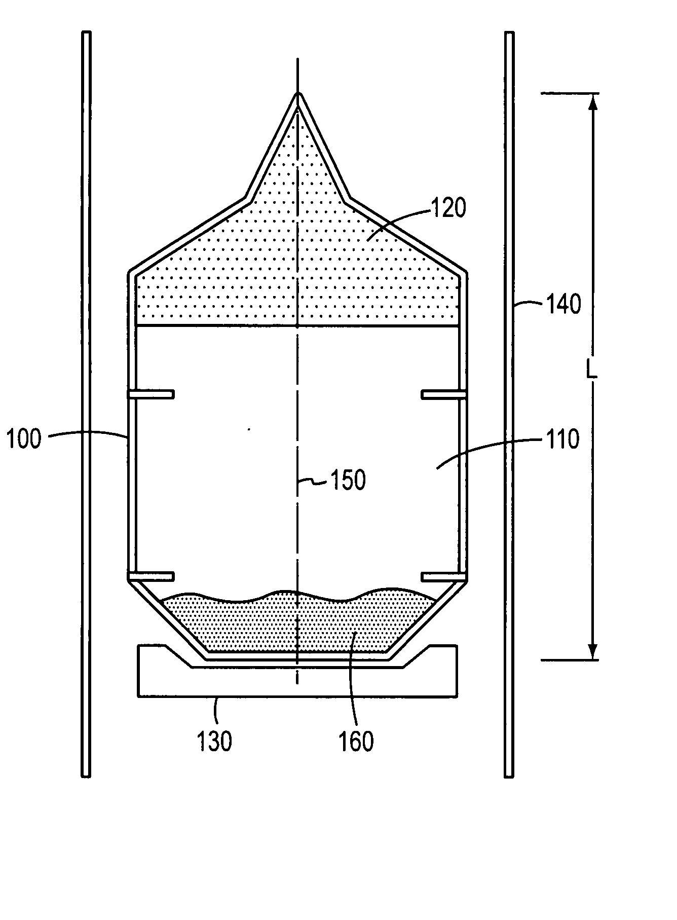
[0006] Microvoids (MVs) in AlN single crystals are a type of crystallographic defect that can be classified as an inclusion. The lateral (i.e. parallel to the c-plane) size of the MV defects typically varies from 0.1 to 3 micrometers (μm). Under low resolution (≦100×) optical microscopy, the MVs appear to be spherically shaped inclusions. However, under higher (≧200×) resolution optical microscopy, as well as when imaged using Atomic Force Microscopy (AFM), the MVs appear to have a hexagonal shape well aligned with (i.e., approximately parallel to) the c-plane. During chemical treatment (chemical etching or chemical-mechanical polishing), MVs intersecting an AlN surface leave shallow pits with a round or hexagonal shape. Also, AlN material with a significant density of MVs tends to etch faster (during chemical etching) than the material with somewhat lower MV density. Therefore, the MVs can behave as heterogeneous inclusions in the AlN solid phase. Th...


PUM

PropertyMeasurementUnit
Temperatureaaaaaaaaaa

Abstract

Reducing the microvoid (MV) density in AlN ameliorates numerous problems related to cracking during crystal growth, etch pit generation during the polishing, reduction of the optical transparency in an AlN wafer, and, possibly, growth pit formation during epitaxial growth of AlN and/or AlGaN. This facilitates practical crystal production strategies and the formation of large, bulk AlN crystals with low defect densities—e.g., a dislocation density below 104 cm−2 and an inclusion density below 104 cm−3 and/or a MV density below 104 cm−3.

Description

CROSS-REFERENCE TO RELATED APPLICATION [0001] The present application claims the benefits of and priority to U.S. Provisional Application Ser. No. 60 / 740,082, filed on Nov. 28, 2005, the entire disclosure of which is hereby incorporated by reference.GOVERNMENT SUPPORT [0002] This invention was made with United States Government support under 70NANB4H3051 awarded by the National Institute of Standards and Technology (NIST). The United States Government has certain rights in the invention.BACKGROUND [0003] Aluminum nitride (AlN) holds great promise as a semiconductor basis material for numerous applications, e.g., opto-electronic devices such as short-wavelength LEDs and lasers, dielectric layers in optical storage media, electronic substrates, and chip carriers where high thermal conductivity is essential, among many others. In principle, the properties of AlN will allow light emission in the 200 nm wavelength region to be achieved. But many practical difficulties should be addressed...

Claims


Application Information

Patent Timeline
IPC IPC(8): H01L21/00
CPCC30B23/00C30B29/403B28D5/00Y10T428/21C30B23/02C30B33/02C30B25/02C30B25/08C30B25/10H01L21/0201H01L21/02389H01L21/0254H01L21/30625C23C16/34C30B25/18
Inventor BONDOKOV, ROBERT T.MORGAN, KENNETHSLACK, GLEN A.SCHOWALTER, LEO J.
Owner CRYSTAL
Why Eureka
Try Eureka