Organic electroluminescent display

an electroluminescent display and electroluminescent technology, applied in the direction of discharge tube luminescnet screen, discharge tube/lamp details, organic semiconductor devices, etc., can solve the problems of oxidation the inability to obtain high-quality image display, and the degraded characteristics of the organic layer or the electron injection layer. achieve high reliability, high efficiency, and high-quality image display

Active Publication Date: 2005-06-16
KIDO JUNJI +1
View PDF9 Cites 49 Cited by
  • Summary
  • Abstract
  • Description
  • Claims
  • Application Information

AI Technical Summary

Benefits of technology

[0029] In the present invention described above, the electron transport protective layer disposed between the first cathode layer and the second cathode layer has a function of preventing degradation or oxidation of the organic layer or the first cathode layer at the time of the forming of the second cathode layer. Moreover, according to the present invention, the electron transport protective layer is disposed between the first cathode layer and the second cathode layer, and the electron transport protective layer contains the alkali metal and/or the alkali earth ...

Problems solved by technology

However, in the conventional organic EL image display apparatus in which the upper surface emission is possible, oxidation of the organic layer or the electron injection layer cannot be avoided by introduction of oxygen in a step of forming the transparent cathode.
Therefore, there have been problems that the characteristics of the organic layer or the electron injection layer are degraded, dark spots are generated, and high-quality image display cannot be obtained.
Moreover, in the conventional organic EL image display apparatus in which the upper surface emission is possible, there have been problems that an impact b...

Method used


Image

  • Organic electroluminescent display
  • Organic electroluminescent display
  • Organic electroluminescent display

Examples


example 1

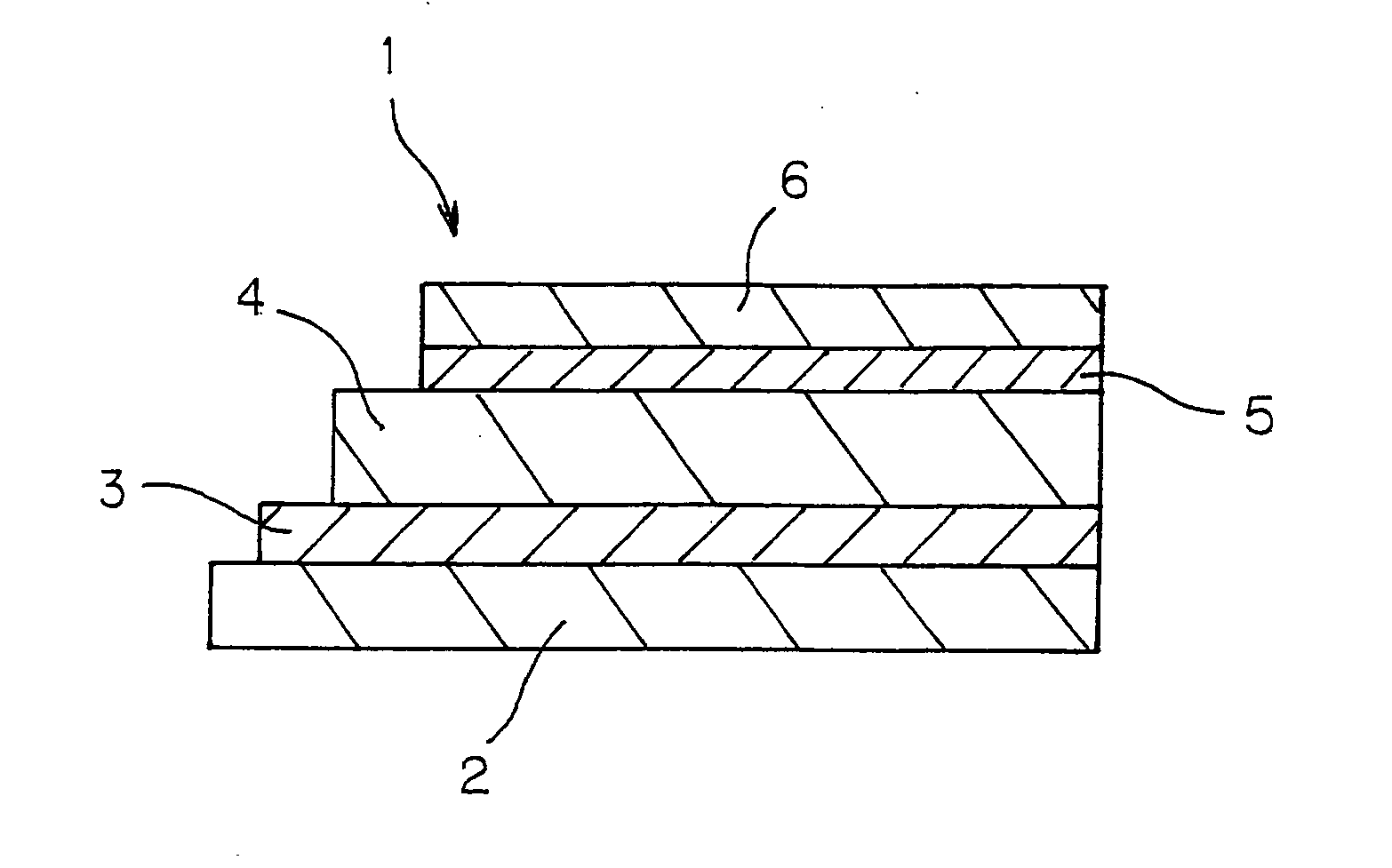
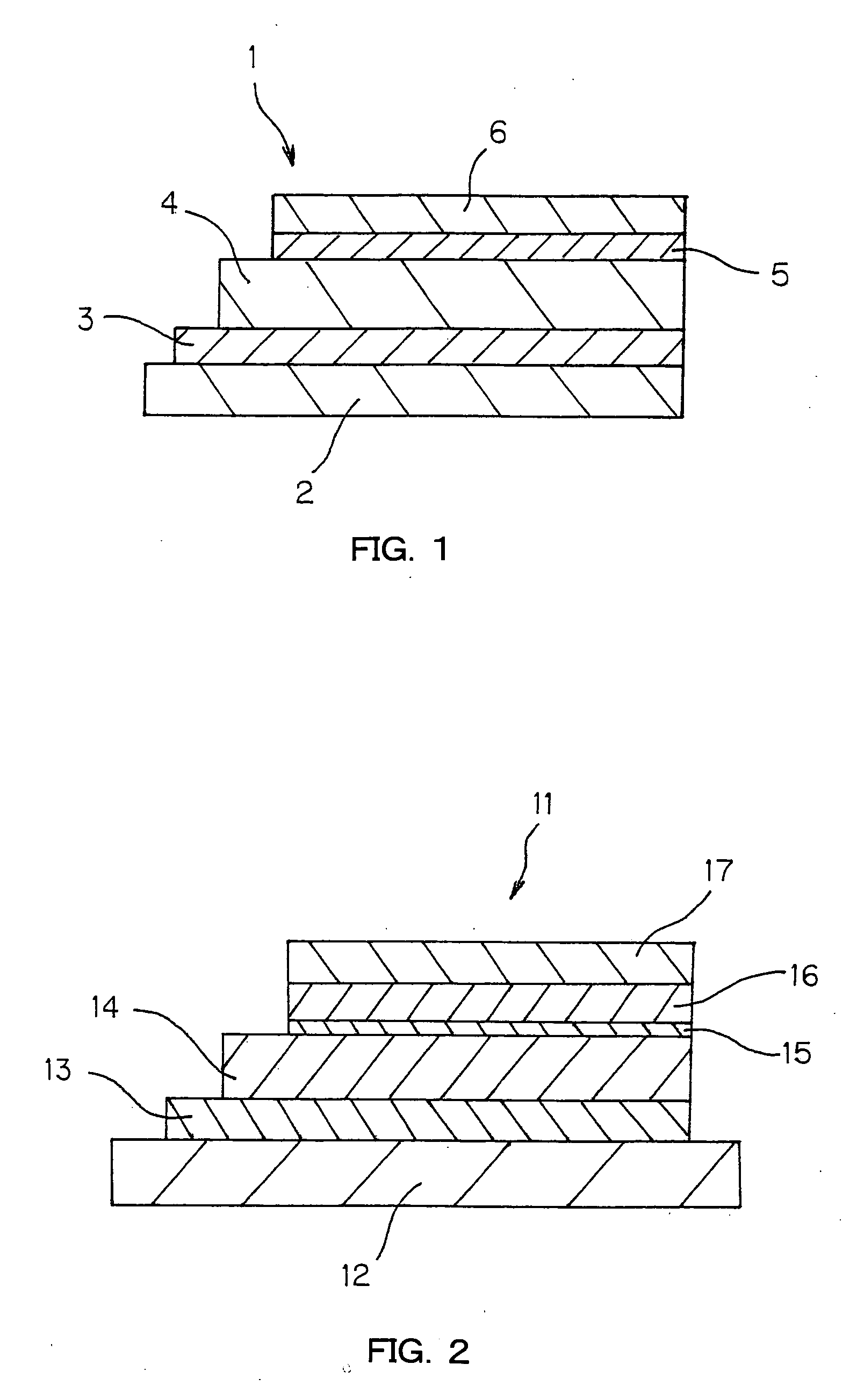
[0087] A transparent glass substrate (nonalkali glass NA35 manufactured by NH Techno Glass K.K.) having a size of 25 mm×25 mm and a thickness of 0.7 mm was prepared as a substrate, this transparent glass substrate was cleaned in accordance with the law, and thereafter an Al thin film (thickness of 100 nm) was formed by a magnetron sputtering method. In the formation of the Al thin film, Ar was used as a sputter gas, and a pressure of 0.15 Pa, and DC output of 200 W were set. Next, to impart a function of promoting the hole injection onto the Al thin film, a thin film of indium tin oxide (ITO) (thickness of 20 nm) was formed by a magnetron sputtering method. In the formation of the ITO thin film, a mixture gas (volume ratio of Ar:O2=100:1) of Ar and O2 was used as the sputter gas, and a pressure of 0.1 Pa and DC output of 150 W were set.

[0088] Next, with respect to the anode layer of the Al thin film and ITO thin film, a low-resistivity meter Loresta-GP (MCP-T600) manufactured by Di...

example 2

[0104] The organic EL display apparatus was prepared in the same manner as in Example 1 except that a ZrN thin film (thickness of 50 nm) was formed as the barrier conductive layer instead of the TiN thin film on the same conditions.

[0105] It is to be noted that as a result of the measurement in the same manner as in Example 1, the surface resistivity of the ITO thin film including the ZrN thin film was 20 Ω / . As a result of the measurement of the moisture-vapor transmission, oxygen transmission rate, specific resistance, and optical transparency in the visible region of 380 to 780 nm of the ZrN thin film in the same manner as in Example 1, the moisture-vapor transmission was 0.3 g / m2 / day, the oxygen transmission rate was 0.2 cc / m2 / day·atm, the specific resistance was 3.4×10⁻⁴ Ω·cm, and the visible region average transparency was about 70%.

[0106] The current density at the time of the application of the voltage of 6 V onto the anode and cathode of the organic EL display apparatus w...

example 3

[0107] The organic EL display apparatus was prepared in the same manner as in Example 1 except that an Au thin film (thickness of 30 nm) was formed as the barrier conductive layer instead of the TiN thin film in a vacuum vapor deposition method (degree of vacuum of 5×10⁻⁵ Pa, film forming rate of 0.5 A / second).

[0108] It is to be noted that as a result of the measurement in the same manner as in Example 1, the surface resistivity of the ITO thin film including the Au thin film was 15 Ω / . As a result of the measurement of the moisture-vapor transmission, oxygen transmission rate, specific resistance, and optical transparency in the visible region of 380 to 780 nm of the Au thin film in the same manner as in Example 1, the moisture-vapor transmission was 0.1 g / m2 / day, the oxygen transmission rate was 0.1 cc / m2 / day·atm, the specific resistance was 1.6×10⁻⁴ Ω·cm, and the visible region average transparency was about 40%.

[0109] The current density at the time of the application of the v...


PUM


Abstract

An organic electroluminescent image display apparatus capable of displaying a high-quality image wherein light is taken out from a cathode layer side of an upper surface is described. The organic electroluminescent image display apparatus includes an anode layer, an organic layer, a barrier conductive layer having optical transparency, and a cathode layer having the optical transparency successively disposed on a substrate. The barrier conductive layer contains a metal, an inorganic nitride, and/or an inorganic oxide. Alternatively, the organic electroluminescent image display apparatus includes an anode layer, an organic layer, a first cathode layer having optical transparency, an electron transport protective layer having the optical transparency, and a second cathode layer having the optical transparency successively disposed on a substrate. The electron transport protective layer contains an alkali metal and/or an alkali earth metal in an electron transporting organic material.

Description

BACKGROUND OF THE INVENTION [0001] The present invention relates to an organic electroluminescent image display apparatus, especially to an organic electroluminescent image display apparatus in which light can be taken out on a cathode layer side of an upper surface. [0002] An organic electroluminescent (EL) device has advantages that visibility is high by self color development, an all-solid display superior in impact resistance is provided different from a liquid crystal display, a speed of response is high, little influence of a temperature change is exerted, and a visual field angle is large. In recent years, use as a light emitting device in an image display apparatus has been noticed. [0003] For a constitution of the image display apparatus using the organic EL device, a constitution is usually employed in which a stacked structure of an anode layer / light emitting layer / cathode layer is basic and a transparent anode layer is formed on a substrate using a glass substrate. In th...

Claims


Application Information

Patent Timeline
IPC IPC(8): H01L51/50H01L51/52H05B33/00
CPCH01L51/5048H01L51/5092H01L2251/5315H01L51/5237H01L51/5221H10K50/14H10K50/171H10K2102/3026H10K59/8052H10K59/873H10K50/82H10K50/844
Inventor MORI, TOSHITAKAOHYAGI, YASUYUKIKIDO, JUNJI
Owner KIDO JUNJI
Why Eureka
Try Eureka