Instruction prefetch-based multi-core shared memory control equipment

A technology for controlling equipment and instruction prefetching, applied in the address formation of the next instruction, instruments, machine execution devices, etc., can solve the problems of low data throughput, increased delay, and large memory access delay, so as to improve transmission efficiency, The effect of reducing time loss and increasing throughput

Inactive Publication Date: 2011-10-05
XIDIAN UNIV
View PDF6 Cites 22 Cited by
  • Summary
  • Abstract
  • Description
  • Claims
  • Application Information

AI Technical Summary

Problems solved by technology

However, the separation and transmission process of the traditional shared bus is complicated and time-consuming. The slave device needs to re-apply to the bus arbitration for data transmission, and then needs to wait until the master device obtains the right to use the bus, and then completes a data transmission through a new bus transmission cycle.
This will increase the delay of the master processor accessing the slave DRAM memory, reduce the data throughput rate, and limit the performance of parallel p

Method used


Image

  • Instruction prefetch-based multi-core shared memory control equipment
  • Instruction prefetch-based multi-core shared memory control equipment
  • Instruction prefetch-based multi-core shared memory control equipment

Examples


Example Embodiment

[0054] Example 1

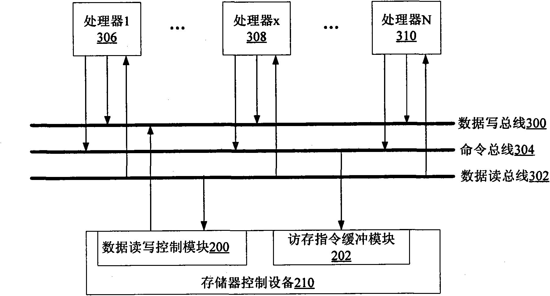
[0055] Such as figure 2 Shown is a schematic diagram of a multi-core shared memory control device based on instruction prefetching. In the embodiment of the present invention, the storage access command and the read and write data are processed separately using different bus structures, so that the parallel execution of the memory access can be realized to the greatest extent. The command bus 304 is a one-way bus, which is only responsible for transmitting memory access instructions sent from multiple processors. In the embodiment of the present invention, the instruction format of the memory access instruction includes the instruction type of this instruction, the processor ID number, the address of the accessed memory, the address of the internal register of the processor, and the number of data to be transferred.

[0056] In order to improve the throughput performance of data, the data bus is divided into a data read bus 302 and a data write bus 300 in the e...

Example Embodiment

[0057] Example 2

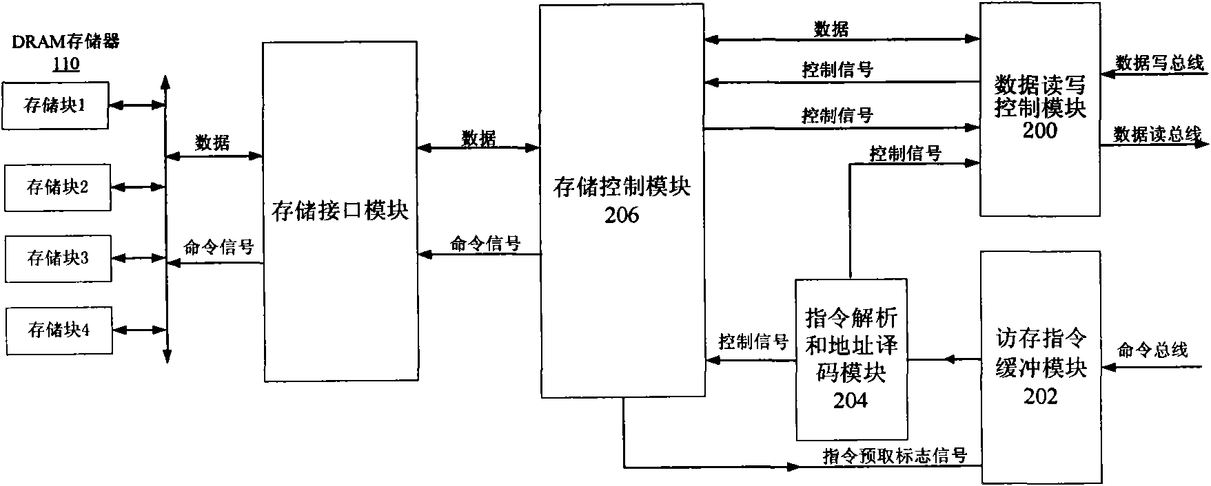
[0058] The storage control device instruction prefetching implementation mode of this embodiment is as follows Figure 4 Shown. The implementation manner involves the storage control module 206, the memory access instruction buffer module 202, and the instruction parsing and address decoding module 204.

[0059] The storage control module 206 includes a read-write control logic 400, a control information register 402, an address comparator 404, and a flag register 406. The read-write control logic 400 is responsible for controlling the jump of the internal state of the storage control device, achieving correct reading and writing of data, and determining when to send the instruction prefetch flag signal 408. The read-write control logic 400 determines the next state according to the information of the current instruction 412 stored in the control information register 402 and the content of the flag register 406. The control information register 402 is responsib...

Example Embodiment

[0085] Example 3

[0086] The DRAM storage control device of the embodiment of the present invention includes a data read and write control module 200. The implementation of the data read and write control module 200 is as follows: Figure 8 Shown. The data read / write control module 200 includes: an internal bus interface 812, which receives control signals from the storage control module 206 and the instruction parsing and address decoding module 204 and data read from the DRAM memory 110, the control signals including memory access instructions Type, processor ID number, designated multi-threaded processor internal register address and data bus request signal; data read bus address data register 806: responsible for saving the address of the designated multi-threaded processor register on the data read bus, data read bus request signal and Data read bus data; data write bus address register 808: responsible for saving the specified multithread processor register address and da...


PUM


Abstract

The invention discloses an instruction prefetch-based multi-core shared memory control equipment. The memory control equipment comprises an access instruction buffer module, an instruction resolving and address decoding module, a data read-write control module, a memory control module and a memory interface module. The data read-write control module controls the transmission of data between a memory and an on-chip multi-core processor. The memory control module generates an instruction prefetch marking signal and fetches a next access instruction from the access instruction buffer module in advance, the next access instruction is pre-decoded through the instruction resolving and address decoding module, and the memory control module dynamically selects a page opening or page closing strategy of the memory according to the control information of the prefetch instruction. The memory control equipment can reduce the delay caused by the access of the processor, improve the transmission efficiency of the data and meet the requirement for high-performance storage bus throughput required when the processors work in parallel.

Description

technical field [0001] The invention relates to a data storage control system, in particular to a multi-core shared memory control device based on instruction prefetching. Background technique [0002] Since the 1980s, processor performance has been doubling every 18 months according to Moore's Law, while memory access latency has only increased by 10% every 12 months on average. The performance gap between processor and memory, namely "memory wall", is getting bigger and bigger, and has become the main consideration of parallel real-time multi-core processing system. [0003] At present, dynamic random access memory (DRAM) has been widely used in the field of data storage. Generally, a DRAM control device is used to control reading and writing of the DRAM. The DRAM control device receives the read / write request from the processor, controls the operation of the DRAM through command analysis, writes data into the DRAM or transmits the DRAM data to the processor. figure 1 S...

Claims


Application Information

Patent Timeline
IPC IPC(8): G06F13/16G06F9/32
Inventor 李康光青郝跃雷理彭毓佳
Owner XIDIAN UNIV
Why Eureka
Try Eureka